Methods for analyzing and adjusting semiconductor device, and semiconductor system

a technology of semiconductor integrated circuits and methods, applied in the field of semiconductor devices, can solve the problems of variable absorbing, difficult measurement of propagation delay in semiconductor integrated circuits, and difficult measurement of propagation delay in semiconductor integrated circuits, and achieve the effect of cost reduction

Active Publication Date: 2010-10-14
NEC CORP
View PDF4 Cites 5 Cited by
  • Summary
  • Abstract
  • Description
  • Claims
  • Application Information

AI Technical Summary

Benefits of technology

[0031]In accordance with the present invention, a unit for measuring a variation in interconnections of a semiconductor integrated circuit device after fabrication need not be provided internally or externally of the semiconductor integrated circuit device. This makes it possible to realize a cost reduction and simplification.

Problems solved by technology

As a result of this adjustment operation, a delay is inserted for the purpose of accommodating for variations in a clock line that drives the semiconductor integrated circuit, thereby causing the variations to be absorbed.
A first problem is that with the methods described in Patent Documents 1 and 2, etc., the measurement of a propagation delay within a semiconductor integrated circuit is very difficult.
Specifically, with regard to a design method for inserting a delay value into a clock line or signal line of a semiconductor integrated circuit after fabrication, thereby accommodating for variations produced at the time of semiconductor fabrication and thus enabling a semiconductor integrated circuit, which would be a fail device in the absence of insertion of the delay value, to be utilized as a pass device, measurement of the propagation delay in the semiconductor integrated circuit is very difficult, in a case where the delay value is decided by measuring an internal or external signal propagation delay value.
Further, although measuring the signal propagation delay value from outside the semiconductor integrated circuit is not as difficult as measuring the propagation delay in the semiconductor integrated circuit, use of an expensive measurement apparatus is required.
A second problem is that taking into consideration the effects of an adjustment value obtained utilizing measurement result, the adjustment is performed up to a target value, where the amount of accommodation for variations becomes smaller than a specified particular value.

Method used


Image

  • Methods for analyzing and adjusting semiconductor device, and semiconductor system
  • Methods for analyzing and adjusting semiconductor device, and semiconductor system
  • Methods for analyzing and adjusting semiconductor device, and semiconductor system

Examples


Embodiment Construction

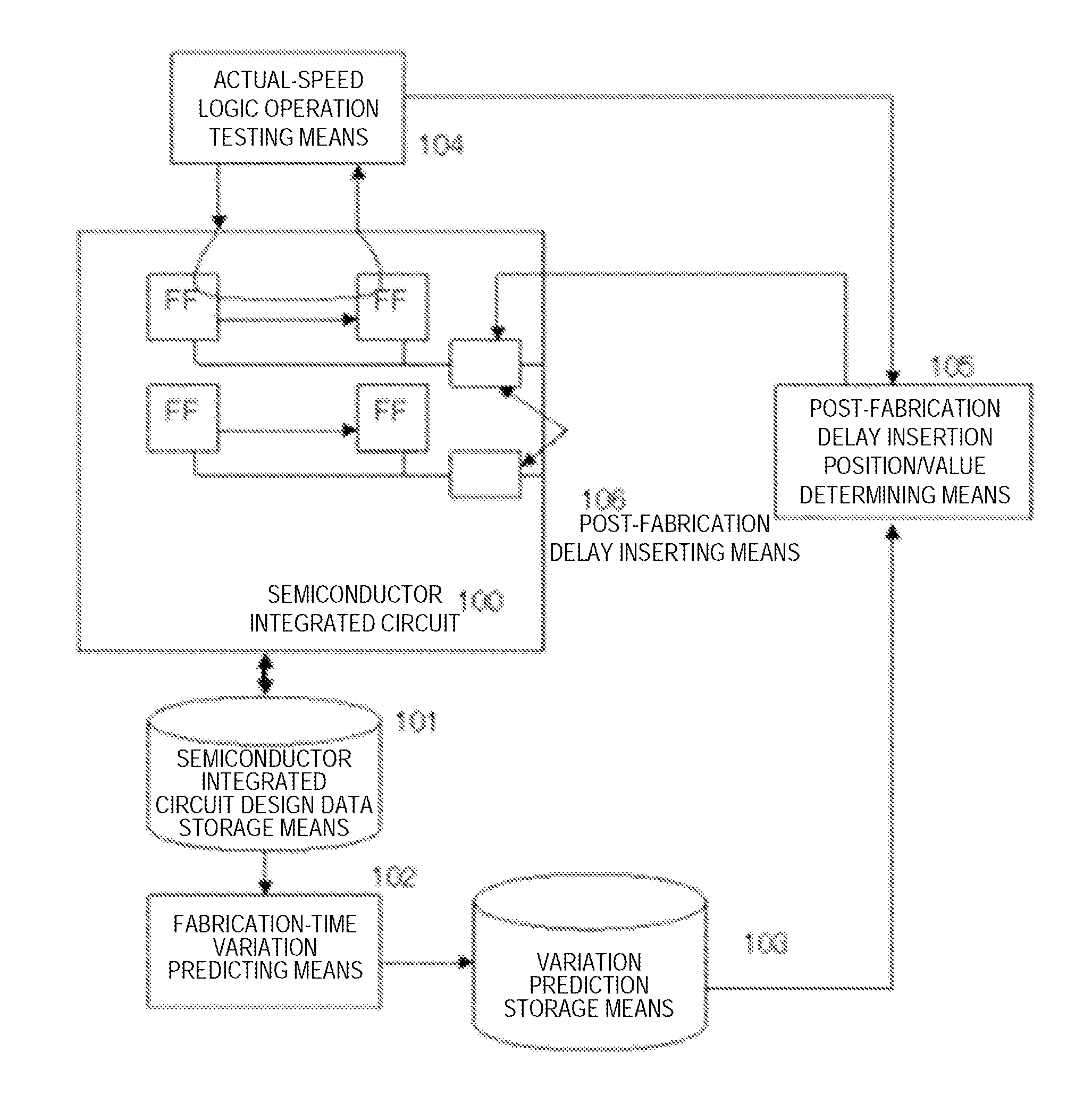
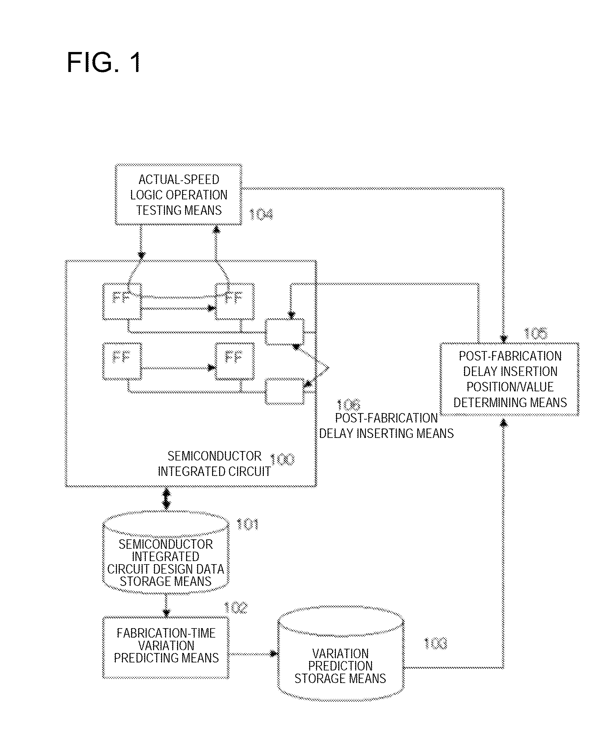
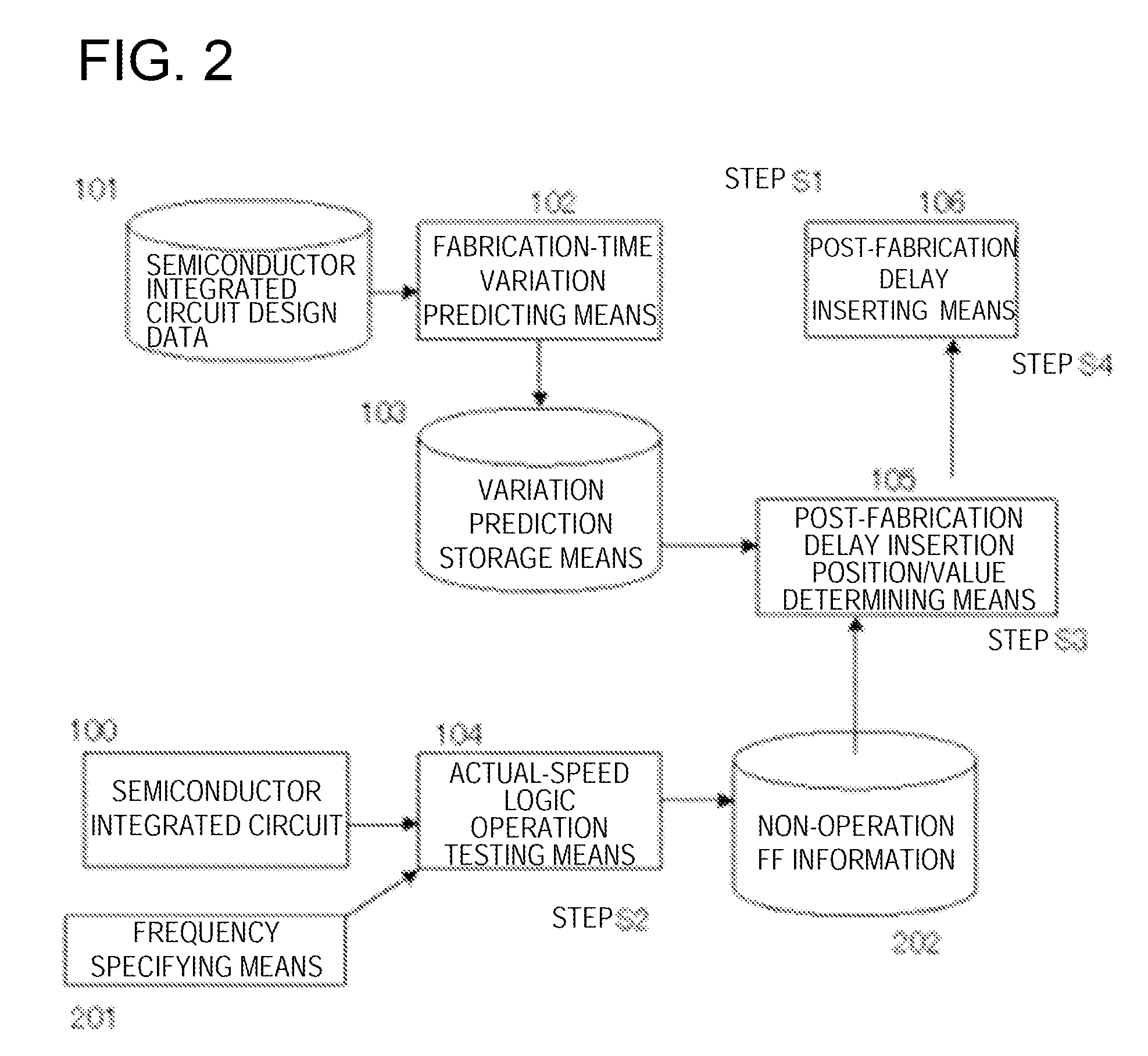
[0042]Exemplary embodiments will now be described with reference to the accompanying drawings for the purpose of describing, in greater detail, the above described present invention above. One of exemplary embodiments of the present invention includes a fabrication-time variation predicting means (unit)(102), a variation prediction storage means (unit)(103), an actual-speed logic operation testing means (unit)(104), a post-fabrication delay insertion position / value determining means (unit)(105) and a post-fabrication delay inserting means (unit)(106). Non-operation of a flip-flop (FF) in a semiconductor device (semiconductor integrated circuit) 100 is computed and predicted beforehand at the time of design prior to fabrication, using the fabrication-time variation predicting means (unit)(102), which predicts that the variation relating to a signal that arrives at the flip-flop (FF) will exceed a particular fixed value, and the result is stored in variation prediction storage means (...


PUM


Abstract

Using fabrication-time variation predicting means that predicts this fact, the variation is predicted beforehand at the design stage prior to fabrication and is stored in variation prediction storage means. Rather than measuring a delay, testing an operation is performed (by a pass/fail determination) by actual-speed logic operation testing means for checking, after fabrication, whether a flip-flop (FF) operates at a specified operation frequency. As a result, the variation is estimated using the non-operation flip-flop (FF) information and the predicted value of the variation from the fabrication-time variation predicting means, and a delay value which corrects for the variation is inserted into a fabricated semiconductor integrated circuit by post-fabrication delay insertion position/value determining means using the variation value that has been estimated.

Description

[0001]This application is the National Phase of PCT / JP2008 / 070885, filed on Nov. 17, 2008, which claims the benefit of previous Japanese Patent Application No. 2007-304900 (filed on Nov. 26, 2007), which is hereby incorporated by reference herein in its entirety.TECHNICAL FIELD[0002]This invention relates to a semiconductor device and, more particularly, to a semiconductor device adjustment method and system in which adjustment of a timing operation is made possible by adjusting delay in the semiconductor device.BACKGROUND ART[0003]As examples of semiconductor integrated circuits in which the timing operation is capable of being adjusted by adjusting a delay in a semiconductor device after its fabrication, thereby enabling a device that has failed to be utilized as a pass device, refer to the descriptions rendered in Patent Documents 1, 2 and Non-Patent Document 1, etc., by way of example. A digital system (clock adjustment method) disclosed in Patent Document 1 includes a semicondu...

Claims


Application Information

Patent Timeline
Patent Type & Authority Applications(United States)
IPC IPC(8): G06F17/50G01R29/02
CPCG01R31/3016G06F11/24G01R31/318525G01R31/31725
Inventor NAKAMURA, YUICHI
Owner NEC CORP
Why Eureka
Try Eureka