
Pocket-enabled chip assembly for implantable devices

a chip and implantable technology, applied in the field of pocket-enabled chip assembly for implantable devices, can solve the problems of inefficient use of surgical site areas, bulky cables, fragile electrode shanks,

Active Publication Date: 2010-10-21
CALIFORNIA INST OF TECH
View PDF10 Cites 37 Cited by
  • Summary
  • Abstract
  • Description
  • Claims
  • Application Information

AI Technical Summary

Benefits of technology

[0026]The foregoing and other objects, aspects, features, and advantages of the invention will become more apparent from the following description and from the claims.

Problems solved by technology

However most suffer from either fragile electrode shanks and bulky cables or inefficient use of surgical site areas.
Among current neural prosthesis technologies, some have well controlled metal electrode fabrication and circuitry integration techniques but have designs that are brittle and difficult to handle.
Some have reliable interconnect cables but are weak on IC expansion capability.
While 3-D integrated silicon probes have been successfully manufactured, the degradation of the signal to noise ratio (SNR) is still a major challenge because electronics are too far away from the recording site.
However, current state of the art technologies still suffer from high signal-to-noise ratio and complicated IC integration schemes.
However, many technologies are still in development and few have actually been transferred to the clinical practice due to constraints in material biocompatibility, device miniaturization, and flexibility.

Method used


Image

  • Pocket-enabled chip assembly for implantable devices
  • Pocket-enabled chip assembly for implantable devices
  • Pocket-enabled chip assembly for implantable devices

Examples


Embodiment Construction

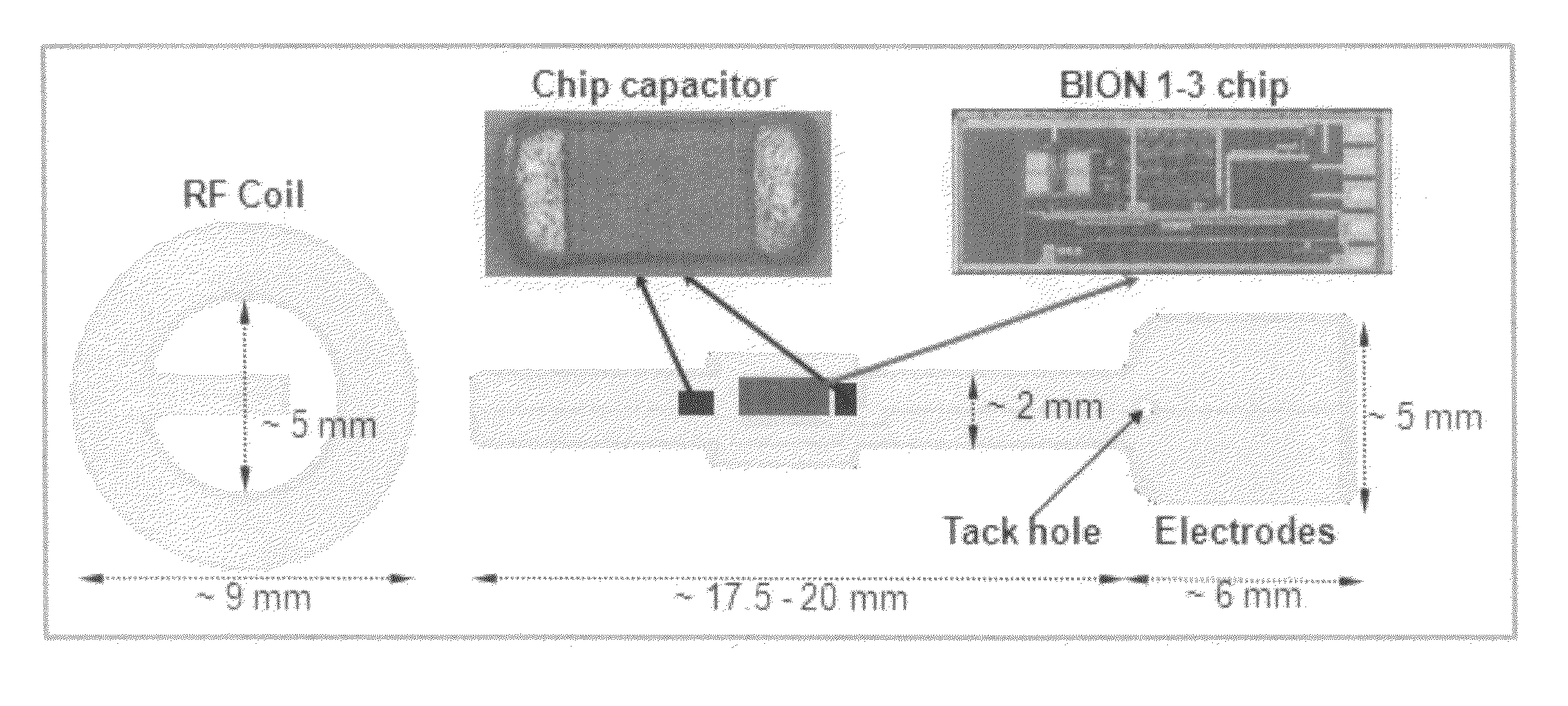
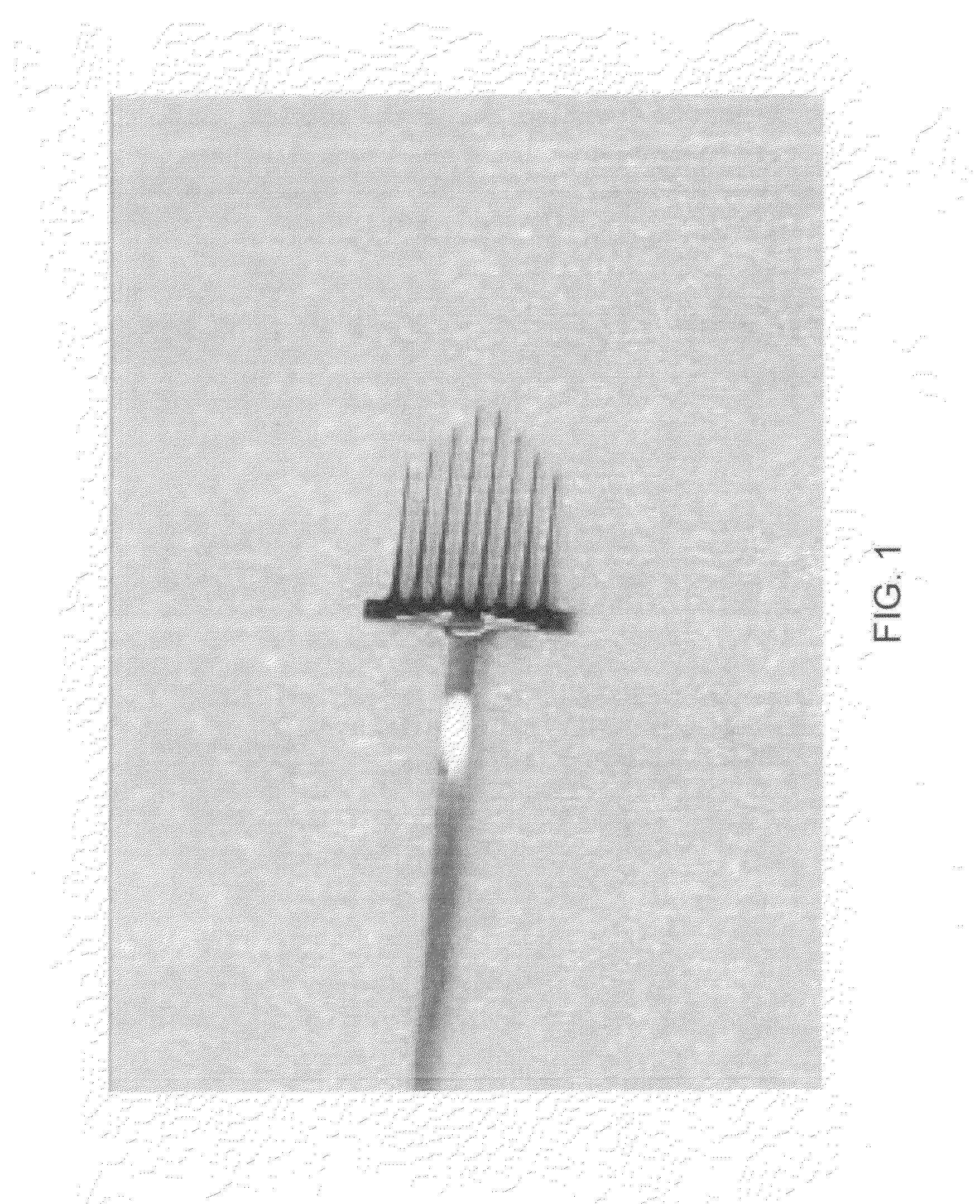
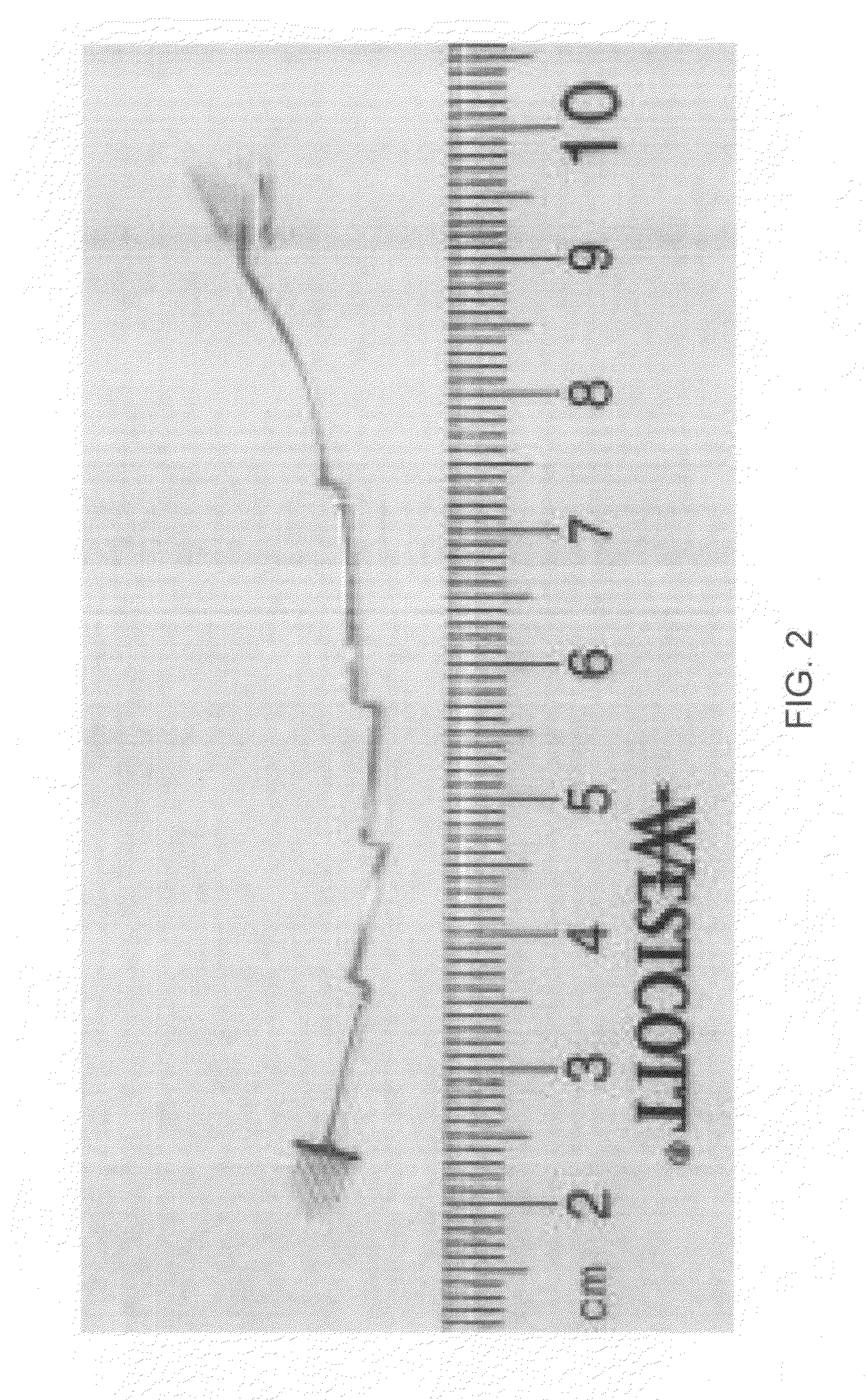
[0085]In this invention, it is believed that the innovation is to use a new “pocket” technology to facilitate the connection and packaging of various different components for use as biomedical implants. To use the technology, pockets (or envelopes) having predesigned sizes to accommodate chips / components, and having pre-metalized electrical connections are made. The chips and correspondent chips / components are then inserted into the pockets with alignment so the metal pads on the pockets and the metal pads on the chips are aligned. Electrical connections between the pockets and the chips / components can be made by applying conductive epoxy or other conductive polymers. These conductive epoxy / polymers can be biocompatible or not, depending on the applications. The end product, however, of this exercise is one or more well connected chips / components on a pocketed substrate or even a completely free-standing flexible substrate, e.g., made of parylene or other polymers. In other terms, a...


PUM

PropertyMeasurementUnit
lengthaaaaaaaaaa
sizeaaaaaaaaaa
impedanceaaaaaaaaaa

Abstract

Systems and methods for providing biologically compatible pockets or envelopes that can contain chips and other circuit elements and can make electrical connection between those elements and living organisms. The assembled biologically compatible pockets and circuit components can have biomedical applications, such as bioimplantable devices such as retinal, cochlear and cortical prosthesis implants, muscular stimulators, and other uses. In various embodiments, the described technology explains how to make and use pocket systems for dealing with chips having connectors on one or two surfaces, and with other circuit components such as resistors, capacitors, inductors and transistors. Operation of chips encapsulated according to the described technology is demonstrated. Accelerated life testing suggests that the pocket systems described will survive for years at 37 degrees C.

Description

CROSS-REFERENCE TO RELATED APPLICATIONS[0001]This application claims priority to and the benefit of co-pending U.S. provisional patent application Ser. No. 61 / 205,490, filed Jan. 21, 2009, which application is incorporated herein by reference in its entirety.STATEMENT REGARDING FEDERALLY FUNDED RESEARCH OR DEVELOPMENT[0002]The U.S. Government has certain rights in this invention pursuant to Grant No. H0031068 awarded by the National Science Foundation.THE NAMES OF THE PARTIES TO A JOINT RESEARCH AGREEMENT[0003]Not ApplicableINCORPORATION-BY-REFERENCE OF MATERIAL SUBMITTED ON A COMPACT DISC[0004]Not ApplicableFIELD OF THE INVENTION[0005]The invention relates to a technology generic for any electronic system assembly involving multiple chips and components, but especially useful for biomedical implants in general and particularly to biomedical implants that employ a chip-in-pocket assembly that allows the total connection and fabrication of a biomedical implant comprising semiconducto...

Claims


Application Information

Patent Timeline
Patent Type & Authority Applications(United States)
IPC IPC(8): H05K7/00H01R43/00
CPCA61B5/6846A61B2562/046Y10T29/49117A61N1/36046A61N1/36032A61B2562/028A61B2562/0209A61N1/375A61B5/04001A61B5/0031A61B5/0478A61N1/36003A61B2562/0215A61N1/36038A61B5/24A61B5/291A61B5/293
Inventor TAI, YU-CHONGHUANG, RAY KUI-JUI
Owner CALIFORNIA INST OF TECH
Learn More