Tiled electroluminescent device with filled gaps

a technology of electroluminescent devices and tiles, applied in the direction of discharge tubes/lamp details, discharge tubes luminescnet screens, electric discharge lamps, etc., can solve the problems of less than satisfactory image quality, large flat-panel displays (e.g. greater than approximately 3 meters in diagonal), and inability to make monolithic substrates. , to achieve the effect of reducing reflection, less visible, and improving light emission uniformity

Active Publication Date: 2010-11-04
GLOBAL OLED TECH
View PDF13 Cites 13 Cited by
  • Summary
  • Abstract
  • Description
  • Claims
  • Application Information

AI Technical Summary

Benefits of technology

[0010]The need is met by a tiled electroluminescent device that improves light-emission uniformity and reduces reflection from ambient light, comprising:
[0013]The present invention has the advantage that the boundaries between adjacent EL devices are less visible when viewed over a large range of viewing angles. An EL device according to the present invention is useful in dark viewing environments, in which the appearance is primarily affected by the light emitted from the device, and in environments with high ambient illumination, in which the appearance is additionally affected by reflected ambient light, and in which the present invention reduces reflections. The present invention can enable the tiling of multiple smaller EL devices into a single, large EL device with improved light emission uniformity, making the appearance of the EL device between tiles consistent with the appearance within tiles. This can enable high-quality, large EL devices for markets such as marketing and large venue communications.

Problems solved by technology

In general, larger displays are more expensive than smaller displays.
Moreover, very large flat-panel displays (e.g. greater than approximately 3 meters in diagonal) cannot be made on a monolithic substrate.
However, such displays typically have visible seams between the tiles, resulting in less than satisfactory image quality.
The optical structures of LCD tiled display systems are typically not well-adapted to the optical structures of area-emissive electroluminescent (EL) devices, such as Organic Light Emitting Diode (OLED) devices, since the use of cross polarizers and liquid crystals modulators within confined light pathways is fundamentally different from the direct modulation and emission of light from EL displays.
Because EL devices employ high-optical-index emissive materials, which emit light into the substrate according to a near Lambertian distribution, a large fraction (e.g. greater than 50%) of the emitted light is typically trapped in the device due to total internal reflection and thus reduces the device efficiency.
However, such overlap area requires that a tile substrate be flexible and non-planar.
However, none of these disclosures address the issue of light leakage between tiles.
Unfortunately, when a display is equipped with such barriers and then viewed at an angle, the absorber can obscure pixels on either side of the black strip, producing a perceptible seam at those angles.

Method used


Image

  • Tiled electroluminescent device with filled gaps
  • Tiled electroluminescent device with filled gaps
  • Tiled electroluminescent device with filled gaps

Examples


Embodiment Construction

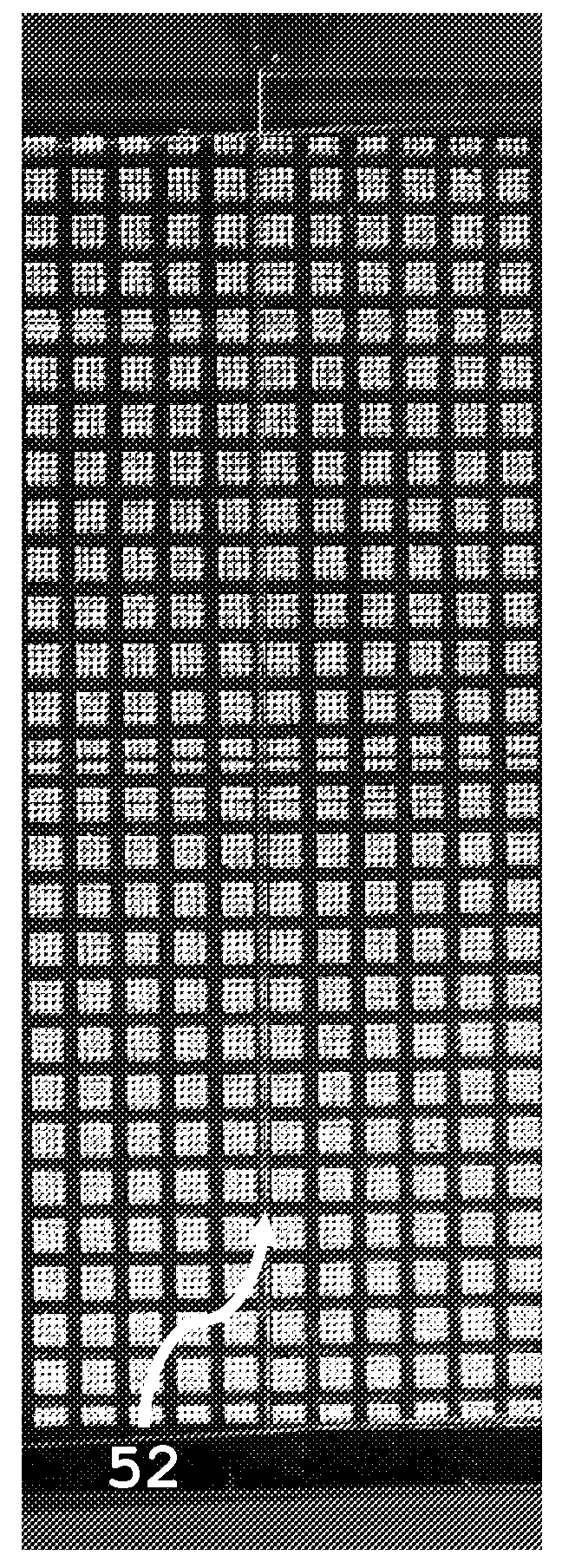
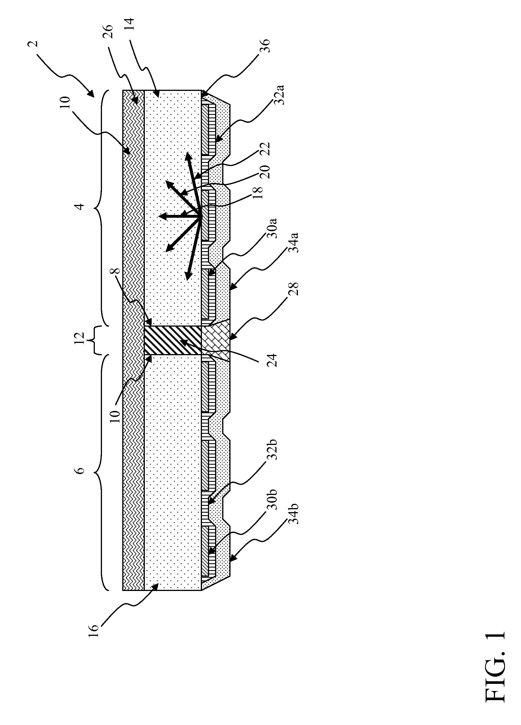
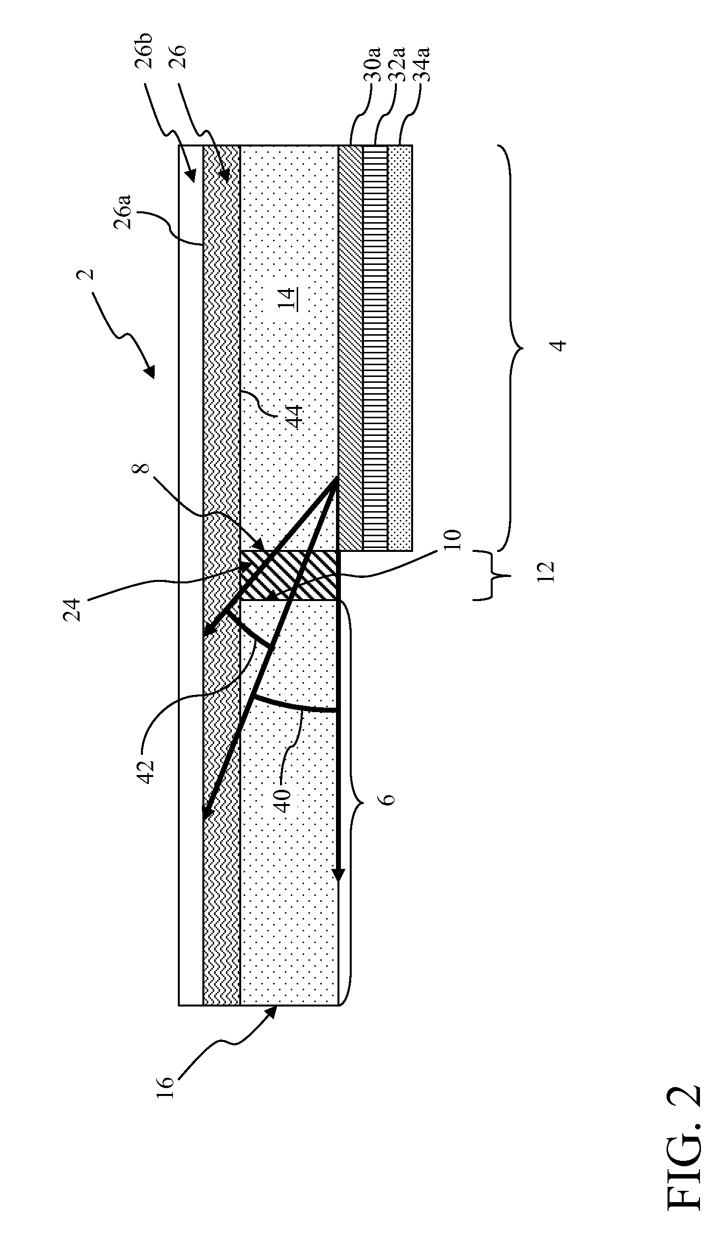
[0022]Referring to FIG. 1, the present invention provides a tiled electroluminescent (EL) device 2 having improved light-emission uniformity and reduced reflection from ambient light. The tiled electroluminescent device 2 includes at least a first 4 and a second 6 electroluminescent device tile. A portion of the edge 8 of the first device tile 4 is abutted with a portion of the edge 10 of the second device tile 6, leaving one or more gap(s) 12 between the first and second device tile edges 8, 10. Each device tile 4, 6 includes a substrate 14, 16, respectively, and at least one electroluminescent diode formed in optical contact with the substrate 14, 16 for emitting light according to a distribution that is substantially Lambertian. By “in optical contact” it is meant that the two materials are not separated by an air gap. As such light is permitted to enter the substrate from the electroluminescent diode and become trapped within this substrate due to total internal reflection betwe...


PUM


Abstract

A tiled electroluminescent device that improves light-emission uniformity and reduces reflection from ambient light includes a first and a second electroluminescent device tile, a portion of the edge of the first device tile abutted with a portion of the edge of the second device tile leaving a gap between the first and second device tile edges, each device tile including a substrate, having an optical index and a level of transparency, and an electroluminescent diode for emitting light according to a distribution that is substantially Lambertian, whereby light is directed along an oblique angle to the surface of the substrate of the first tile and through the edge of the first device tile; and a filler located in the gap between the abutting edges of the first and second device tiles, the filler having an optical index and a level of transparency matched to the substrates.

Description

FIELD OF THE INVENTION[0001]The present invention relates to area-emissive LED flat-panel devices including multiple tiles. Specifically, the present invention relates to improving light emission uniformity of EL flat panel display systems and reducing reflection from ambient light.BACKGROUND OF THE INVENTION[0002]Electronic display systems are commonly used to display information, especially information containing motion or providing interactivity. Typical display systems range in size from small displays used in mobile devices to very large displays visible to thousands of viewers. In general, larger displays are more expensive than smaller displays. Moreover, very large flat-panel displays (e.g. greater than approximately 3 meters in diagonal) cannot be made on a monolithic substrate. Such very large displays are typically made by either positioning individual point-source light-emitting diodes into a large backplane or by tiling smaller displays together. For example, video wall...

Claims


Application Information

Patent Timeline
Patent Type & Authority Applications(United States)
IPC IPC(8): H01J1/64
CPCH01L27/3293H01L51/5281H01L51/5237H10K59/18H10K50/8423H10K50/86H10K59/00
Inventor COK, RONALD S.HAMER, JOHN W.MILLER, MICHAEL E.
Owner GLOBAL OLED TECH
Why Eureka
Try Eureka