LED with enhanced light extraction

a technology of enhanced light and light extraction, which is applied in the direction of basic electric elements, semiconductor devices, electrical equipment, etc., can solve the problems of spontaneous emission of light and light emitting diodes, and achieve the effects of improving light extraction, improving light extraction, and improving non-symmetrical emission

Active Publication Date: 2010-11-11
LUMILEDS HLDG BV
View PDF8 Cites 37 Cited by
  • Summary
  • Abstract
  • Description
  • Claims
  • Application Information

AI Technical Summary

Benefits of technology

[0033]In another preferred implementation of the invention, the light extraction capabilities of the ELEE elements are further improved by disposing scattering elements inside the FLEE elements. These may comprise one or more of colloids, nanospheres, nanorods or nanoclusters.
[0034]In another modification to the present invention, the mesa side walls of the light emitting device are textured to improve light extraction. In one embodiment the mesa texturing is only introduced on two parallel facing sides. This enables improved non-symmetrical emission and accentuates the ellipticity of the profile in the azimuthal axis of the light emitting device, even wh

Problems solved by technology

Light emitting diodes typically suffer from poor light extraction due to the high refractive inde

Method used


Image

  • LED with enhanced light extraction
  • LED with enhanced light extraction
  • LED with enhanced light extraction

Examples


Embodiment Construction

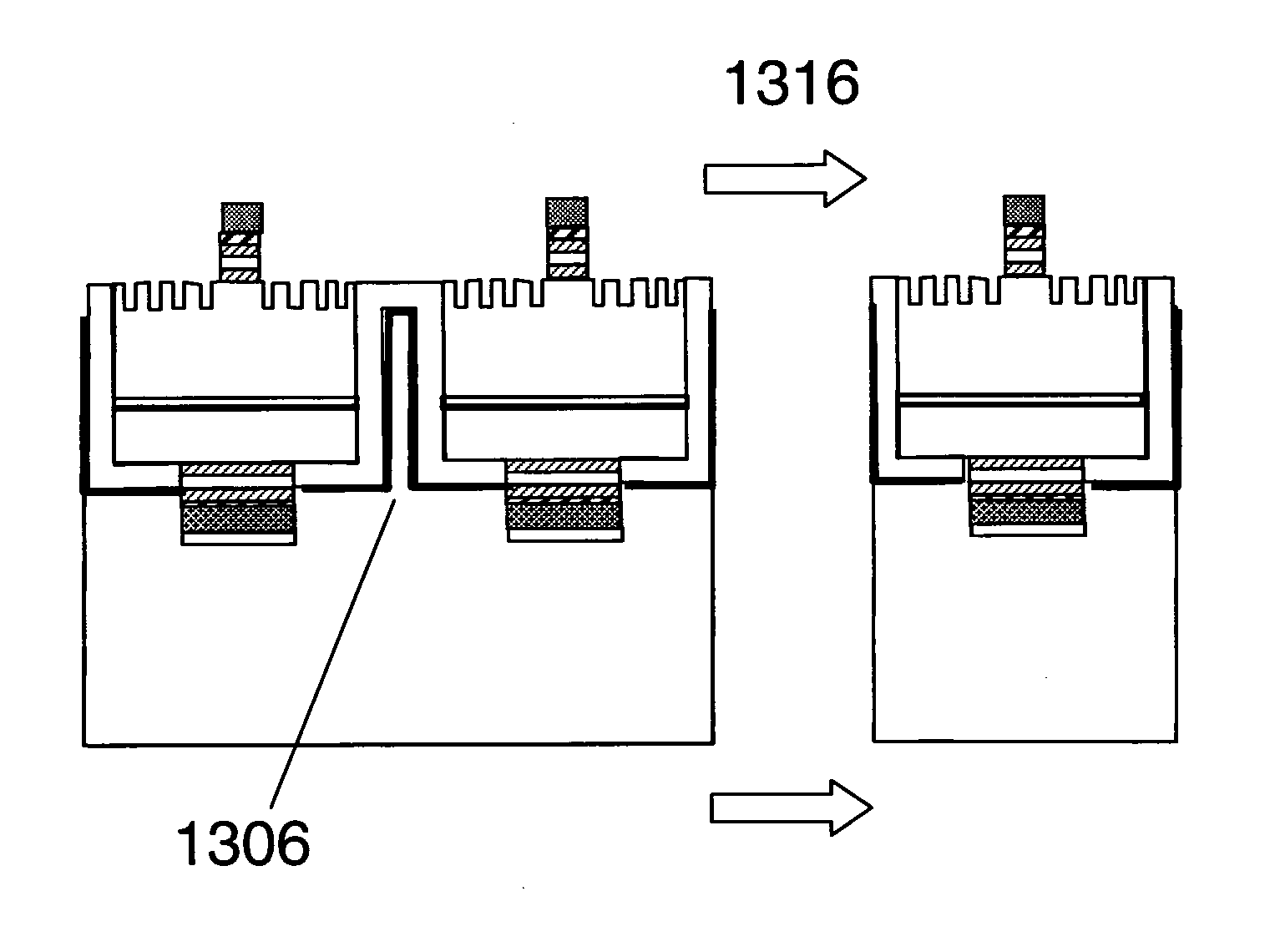
[0067]The object of the invention is to provide a high luminous output semiconductor light emitting device while still maintaining high wall plug efficiency. The invention can be incorporated in a light emitting device fabricated from any semiconductor material system, such as, but not restricted to, InGaN, InGaP, InGaAs, InP, and ZnO. A GaN based light emitting diode (LED) having an epitaxial layer formed on a sapphire substrate is used as an example for illustrating the present invention. However, the present invention is not restricted to epitaxial layers grown on sapphire and may include Si, SiC, Ge, native free-standing GaN, AlN, LiAlO or any other growth and substrate technology. Another object of the invention is the use of LEDs with a vertical current path, in which the electrical current through the p and n doped materials is applied through substantially parallel contacts that allow the current to flow in a vertical direction through the LED structure. These LED structures...


PUM


Abstract

A light emitting device having a plurality of light extracting elements defined on an upper surface of a semiconductor layer of the device, wherein the light extracting elements are adapted to couple light out of the device and to modify the far field emission profile of the device. Each element comprises an elongate region having a length at least twice its width and also greater than the effective dominant wavelength of light generated in the device. The elongate region extends orthogonal to the upper surface but not into the light emitting region of the device and may be oriented at an angle of less than 45° relative to one of a pair of basis axis defining a plane parallel to the semiconductor layer. Each elongate region is spatially separated from neighbouring elongate regions such that it perturbs light generated in the light emitting region independently of the neighbouring regions.

Description

FIELD OF THE INVENTION[0001]The present invention relates to Light Emitting Devices and Light Emitting Diodes (LEDs) having surface patterning for improved light extraction and far field profile and to a method of manufacturing the devices.BACKGROUND TO THE INVENTION[0002]Light emitting devices and diodes are based on a forward biased p-n junction. LEDs have recently reached high brightness levels that have allowed them to enter into new solid state lighting applications as well as replacements for high brightness light sources such as light engines for projectors and automotive car headlights. These markets have also been enabled by the economical gains achieved through the high efficiencies of LEDs, as well as reliability, long lifetime and environmental benefits. These gains have been partly achieved by use of LEDs that are capable of being driven at high currents and hence produce high luminous outputs while still maintaining high wall plug efficiencies.[0003]Solid state lightin...

Claims


Application Information

Patent Timeline
IPC IPC(8): H01L33/10H01L33/02H01L21/02H01L33/00H01L33/20H01L33/22
CPCH01L33/0079H01L2933/0091H01L33/22H01L33/20H01L33/0093
Inventor MCKENZIE, JAMES STUARTZOOROB, MAJD
Owner LUMILEDS HLDG BV
Why Eureka
Try Eureka