Asynchronous nano-electronics

a nano-electronics and asynchronous technology, applied in the field of asynchronous circuits comprising nanotechnology, can solve the problem that synchronous flexible processors cannot be buil

Inactive Publication Date: 2010-11-11
CALIFORNIA INST OF TECH
View PDF5 Cites 4 Cited by
  • Summary
  • Abstract
  • Description
  • Claims
  • Application Information

AI Technical Summary

Benefits of technology

[0010]In one aspect, the invention relates to an asynchronous nanoelectronic circuit configured to operate according to quasi-delay insensitive principles. The circuit comprises a compute tile having an n-plane, a p-plane and a routing plane, the compute tile including at least a first logic element and a second logic element, the first logic element having at least a first input and at least a first output, the second logic element having at least a second input and at least a second output, the first input and the second input each configured to receive an input signal, the first output and the second output each configured to be connected to one of a high reference voltage via a pullup element a

Problems solved by technology

Synchronous flexible processors cannot be built, since bending the material on which a chip is fabricated causes unpredi

Method used


Image

  • Asynchronous nano-electronics
  • Asynchronous nano-electronics
  • Asynchronous nano-electronics

Examples


Embodiment Construction

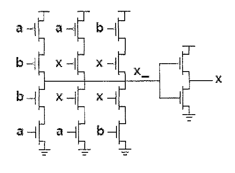
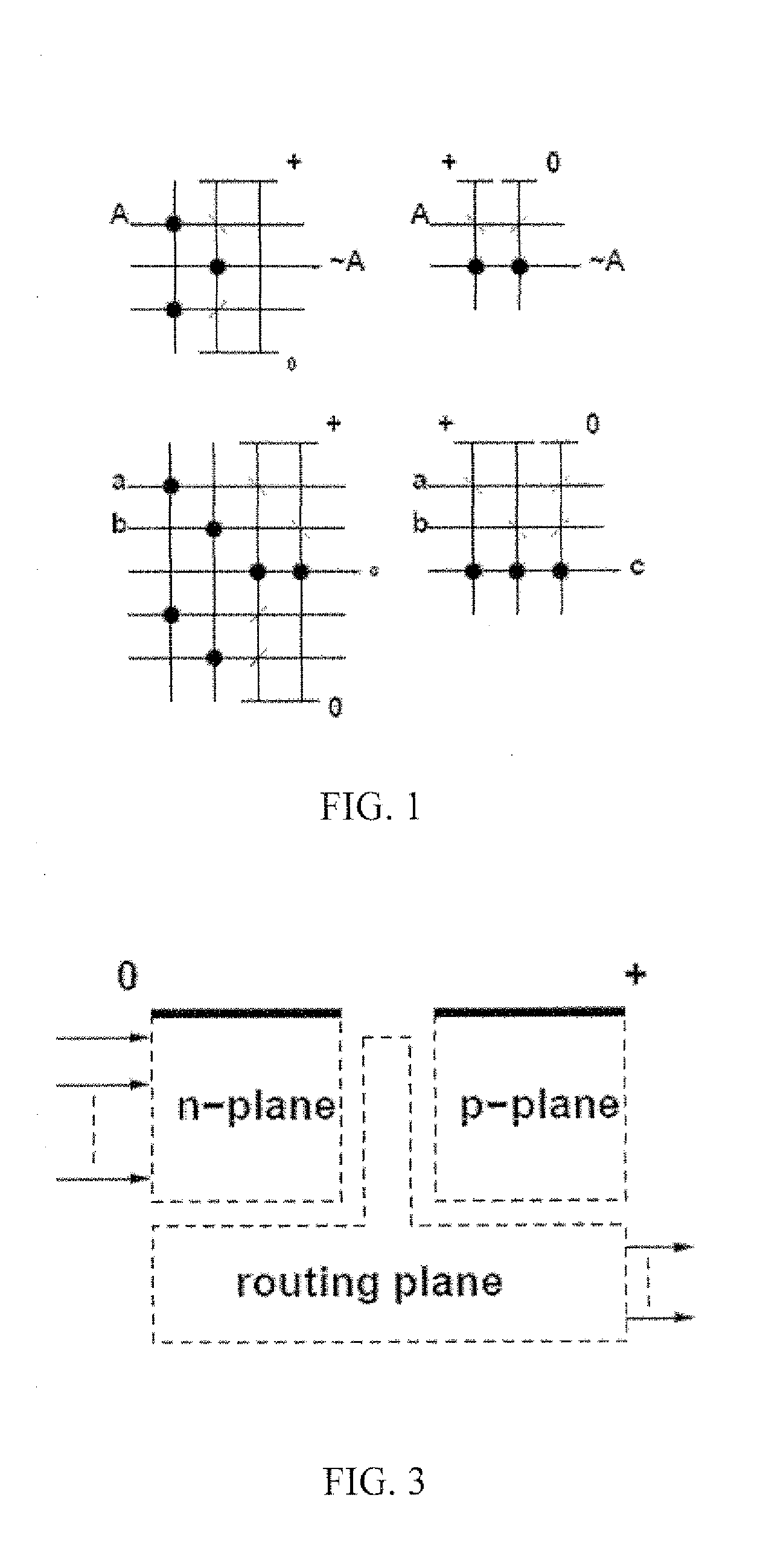
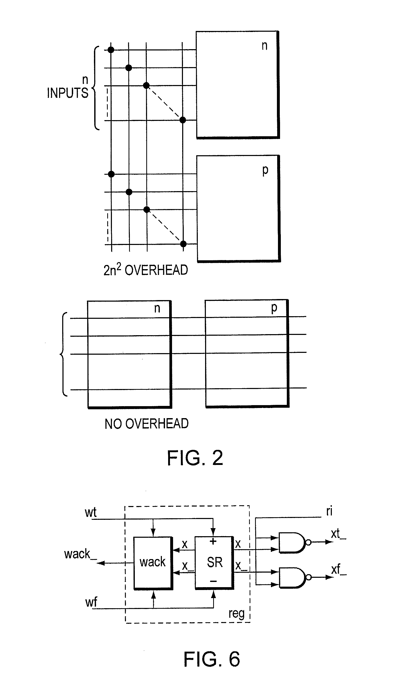
[0029]Currently, molecular nanoelectronics is considered a plausible successor to CMOS. It is a mostly non-lithographic bottom-up fabrication technology based on self-assembly of arrays of silicon nanowires (NW) or carbon nanotubes (CNT), whose main potential advantage at the moment is its density. Great parameter variations and high defect rates should be anticipated for this technology, as should be expected for all nanoscale technologies. Because of the expected variations in specimens, timing should be expected to be difficult to control and predict. Molecular nanowires will be short, precluding the implementation of a global clocking network directly in nanoelectronics. In addition, for extremely high densities of electronic elements, the provision of timing signals consumes a great deal of real estate on a chip. Consequently, asynchronous logic is expected to be an ideal, and probably unavoidable choice, for the design of digital circuits in this technology. We discuss impleme...


PUM


Abstract

Asynchronous nanoelectronic circuits that operate according to principles of quasi-delay insensitive design are described. Circuit or logic elements comprising n-type devices are fabricated in a first n-plane, p-type devices are fabricated in a p-plane, and connections are formed in a routing plane of a compute tile. A state-holding element comprising a selected one of a C-element, a precharge function-block, and a read-write register is described. The state-holding element can hold a value of an output of a logic element during a time when the output is disconnected from a reference voltage. Isochronic forks having an adversary path designed to make state transitions safe are explained.

Description

CROSS-REFERENCE TO RELATED APPLICATIONS[0001]This application claims priority to and the benefit of co-pending U.S. provisional patent application Ser. No. 60 / 858,859, filed Nov. 14, 2006, which application is incorporated herein by reference in its entirety. U.S. patent application Ser. No. 11 / 375,390 filed Mar. 14, 2006 is a related application, which application is incorporated herein by reference in its entirety.STATEMENT REGARDING FEDERALLY FUNDED RESEARCH OR DEVELOPMENT[0002]The U.S. Government has certain rights in this invention pursuant to Grant No. CCF0541461 awarded by the National Science Foundation.FIELD OF THE INVENTION[0003]The invention relates to asynchronous circuits in general and particularly to asynchronous circuits comprising nanotechnology.BACKGROUND OF THE INVENTION[0004]Asynchronous circuits operate without a clock. Quasi Delay Insensitive (hereinafter “QDI”) circuits are a class of delay-insensitive asynchronous circuit which are invariant to (and make no a...

Claims


Application Information

Patent Timeline
IPC IPC(8): H03K19/003
CPCB82Y10/00H01L27/0207H01L29/413H01L29/0673H01L27/11807
Inventor MARTIN, ALAIN J.PRAKASH, PIYUSH
Owner CALIFORNIA INST OF TECH
Why Eureka
Try Eureka