Chain/leapfrog circuit topologies and tools for carbon nanotube / graphene nanoribbon nanoelectronics, printed electronics, polymer electronics, and their confluences

a carbon nanotube and graphene nanoribbon technology, applied in the field of nanoelectronics, nanoelectronics, semiconducting polymer electronics, and printed electronics, can solve the problems of unrealized commercial promise of nanoelectronics, lack of viable analog capabilities for interfacing nanosensors and nanoactuators with “outside world, and complex fabrication, etc., to facilitate the use of traditional scale printed electronics

Active Publication Date: 2010-12-02
GULA CONSULTING LLC
View PDF23 Cites 5 Cited by
  • Summary
  • Abstract
  • Description
  • Claims
  • Application Information

AI Technical Summary

Benefits of technology

[0043]In an embodiment, the invention facilitates the use of traditional scale printed electronics as an emulation tool for chain / leapfrog topology nanoelectronics circuits.

Problems solved by technology

Even in isolation, nanoelectronics is an area of great unrealized commercial promise.
Despite these promising advancements, there are at least five problems holding back the development of systems comprising nanoelectronics for commercial applications:The lack of viable analog capabilities for interfacing nanosensors and nanoactuators with “outside world” and nanosystem-internal digital nanoelectronics (for example, in the 2006 IBM nanotransistor ring oscillator reported in “An Integrated Logic Circuit Assembled on a Single Carbon Nanotube,” Z. Chen et al., Science, Mar. 24, 2006, Vol 311, pp.
Although field-emission nanotriode differential amplifiers comprising carbon nanotube emission elements have been modeled and demonstrated, these devices are larger in physical scale than companion nanoelectronic components, require complex fabrication, and appear difficult to integrate with other types of nanoelectronic components.
Additionally, there is an internal interconnection and a component placement problem for nanocircuits comprising moderate to large numbers of nanotransistors.
However, there are additional problems of concern that provide barriers to commercialization of nanoelectronics.
One of these additional problems is that the techniques for designing and layout of carbon nanotube circuits are not extendable to other types of nanotransistors and molecular transistors.
Another of these additional problems is that the aforementioned specialized physics, models, and many of the above limitations make it difficult for broader populations of circuit designers to conceive of meaningful circuits and systems they could design.
Yet another of these additional problems is that prototyping of nanoelectronic circuits in general can be very difficult, time consuming, and expensive.
The specialized physics, models, and many of the above limitations tend to isolate numerical simulation models to a precious few specialists and specialized isolated software programs.
Further, the aforementioned fabrications costs and design barriers make physical prototyping out of reach for even most of the privileged few of the precious few specialists with access to the aforementioned rarefied and elite R&D funding opportunities.

Method used


Image

  • Chain/leapfrog circuit topologies and tools for carbon nanotube / graphene nanoribbon nanoelectronics, printed electronics, polymer electronics, and their confluences
  • Chain/leapfrog circuit topologies and tools for carbon nanotube / graphene nanoribbon nanoelectronics, printed electronics, polymer electronics, and their confluences
  • Chain/leapfrog circuit topologies and tools for carbon nanotube / graphene nanoribbon nanoelectronics, printed electronics, polymer electronics, and their confluences

Examples


Embodiment Construction

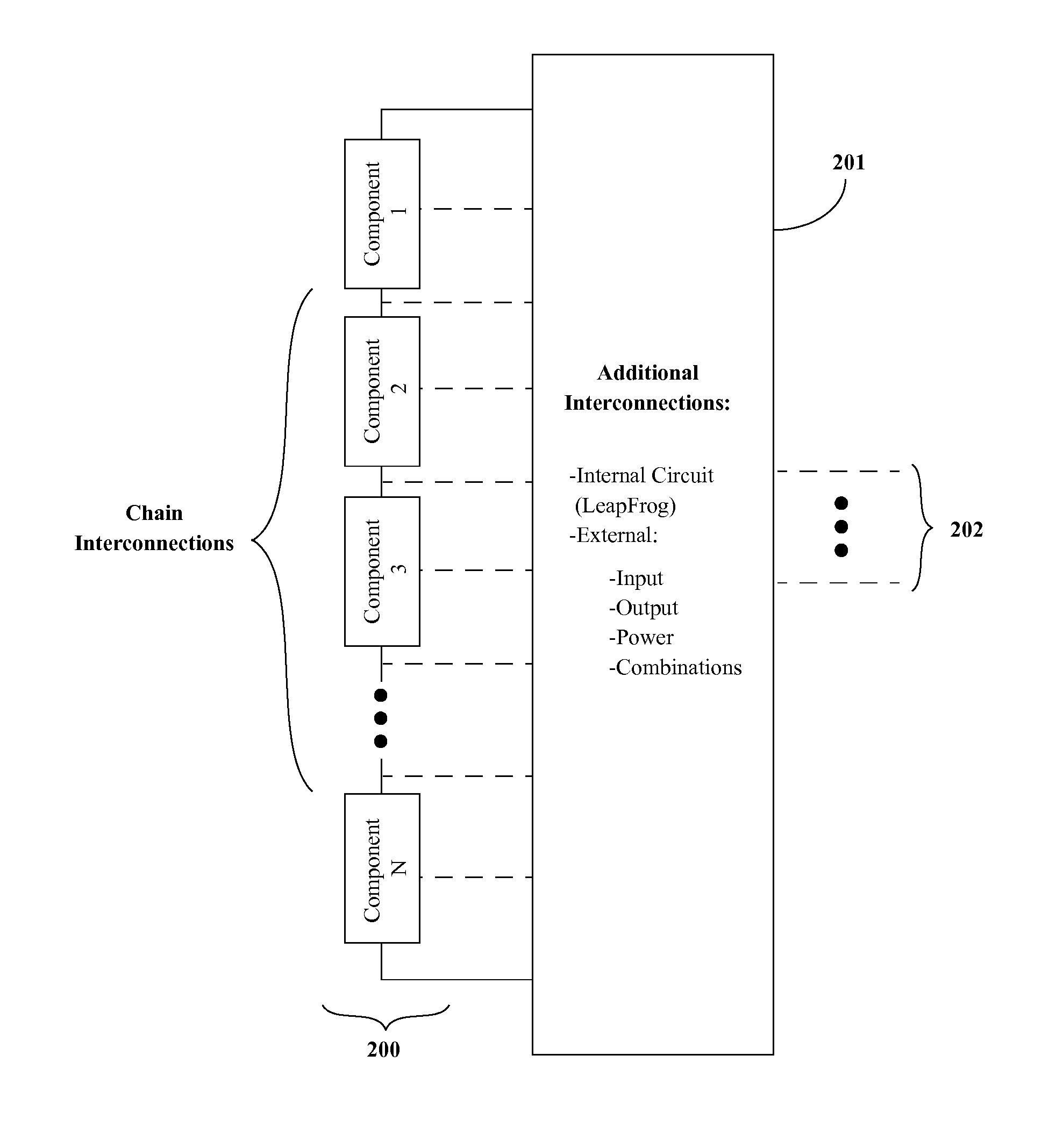
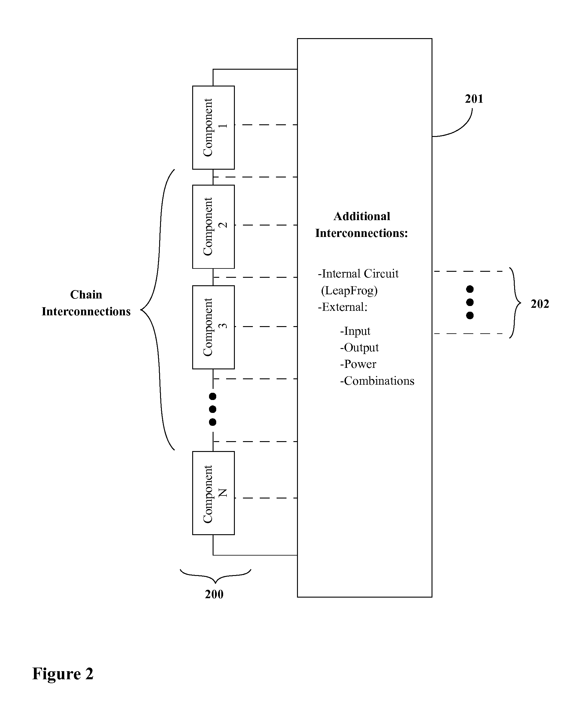
[0078]In the following detailed description, reference is made to the accompanying drawing figures which form a part hereof, and which show by way of illustration specific embodiments of the invention. It is to be understood by those of ordinary skill in this technological field that other embodiments can be utilized, and structural, electrical, as well as procedural changes can be made without departing from the scope of the present invention. Wherever possible, the same element reference numbers will be used throughout the drawings to refer to the same or similar parts.

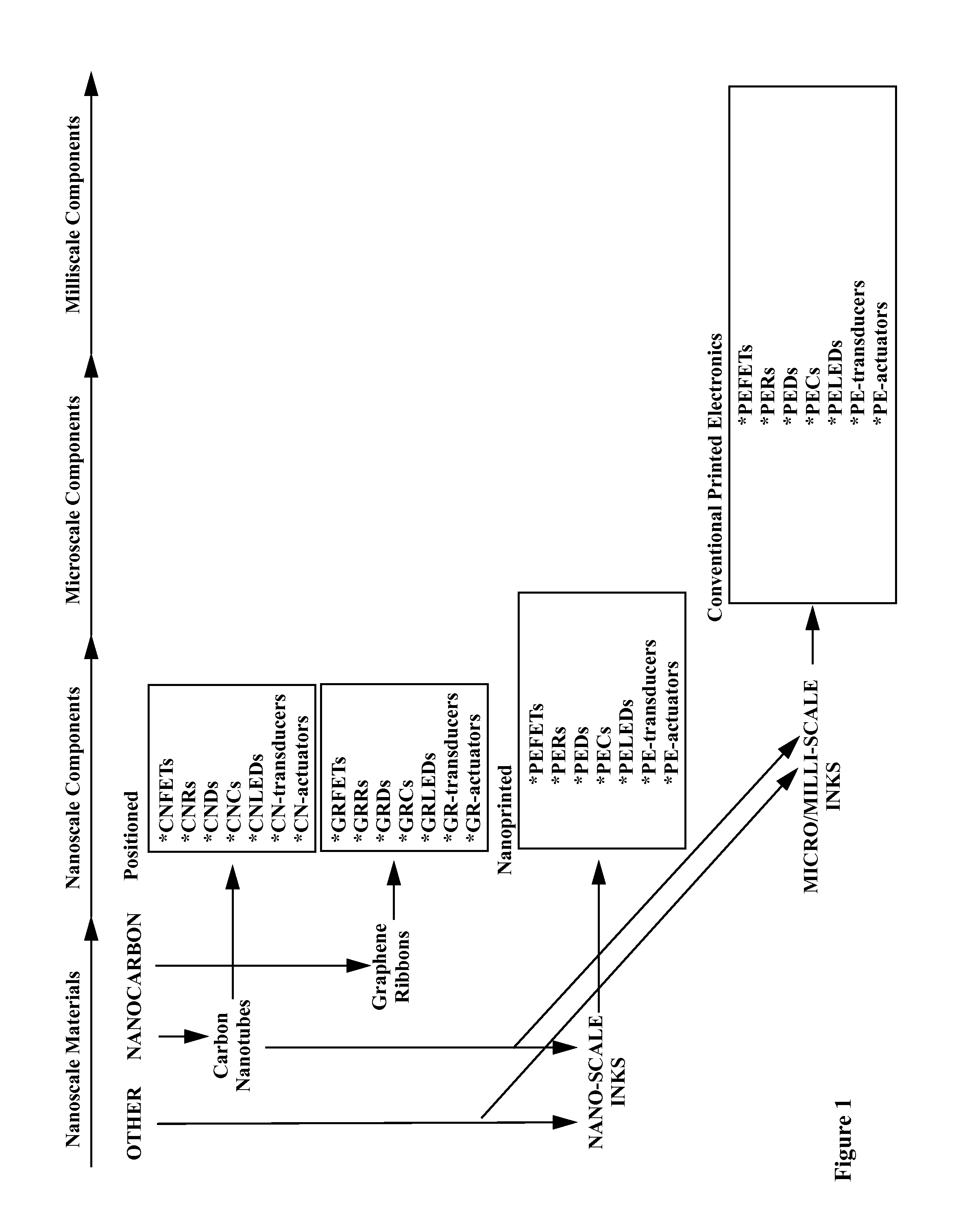
[0079]The present invention addresses these three additional problems with (1) methods and (2) software-based systems for executing on one or more computers. These methods and software-based systems leverage one or more of:[0080]Use of field effect transistors that can be readily fabricated from placement of an insulated conductor proximate to the strip, tube, or ribbon of semiconducting material arranged to span th...


PUM


Abstract

Software for designing and testing types of nanoelectronic circuits and larger scale electronics renderings is described. The software designs circuits comprising only a chain/leapfrog topology. The chain/leapfrog topology permits a wide range of circuits and circuit modules to be implemented on a common shared carbon nanotube, graphene nanoribbon, or strips of other types of semiconducting material, for example as rendered in traditional printed electronics and nanoscale printed electronics or as employing semiconducting polymers. In one approach a chain/leapfrog topology circuit design software tool accesses information in a library of chain/leapfrog circuits data, and creates descriptive data pertaining to a number of approaches to rendering electronics components using a library of component data. The chain/leapfrog circuits data library includes designs for a number of different types of chain/leapfrog circuit modules. The software provides for “IP cores,”“System-on-a-Nanotube,” and other related modular design approaches.

Description

CROSS-REFERENCE TO RELATED APPLICATIONS[0001]This application claims benefit of priority of U.S. provisional application Ser. No. 61 / 217,535 filed on Jun. 1, 2009, incorporated herein by reference. This application is also related to co-pending U.S. patent applications U.S. Ser. No. 12 / 025,562 with a priority date of Feb. 5, 2007, U.S. Ser. No. 12 / 033,212 with a priority date of Feb. 17, 2007, and U.S. 61 / 348,366 with a priority date of May 26, 2010.BACKGROUND OF THE INVENTION[0002]1. Field of the Invention[0003]The present invention generally relates to nanotechnology, nanoelectronics, semiconducting polymer electronics, and to printed electronics at the nanometer, micrometer, and millimeter scale, and in particular, to circuits created from carbon nanotubes, graphene nanoribbons, strips of semiconducting polymers, and semiconducting inks used in printed electronics.[0004]2. Background of the Invention[0005]Even in isolation, nanoelectronics is an area of great unrealized commercia...

Claims


Application Information

Patent Timeline
Patent Type & Authority Applications(United States)
IPC IPC(8): G06F17/50
CPCG06F17/5045G06F30/30
Inventor LUDWIG, LESTER F.
Owner GULA CONSULTING LLC
Why Eureka
Try Eureka