Parallel electron beam lithography stamp (PEBLS)

a lithography stamp and electron beam technology, applied in the field of parallel electron beam lithography stamps, can solve the problems of limiting the speed of production, affecting the accuracy of lithography,

Inactive Publication Date: 2009-06-23
MOUTTET BLAISE LAURENT
View PDF16 Cites 0 Cited by
  • Summary
  • Abstract
  • Description
  • Claims
  • Application Information

AI Technical Summary

Problems solved by technology

However, these techniques are limited by the wavelengths of the light used and fabrication below 100 nm is problematic.
Electron and ion beam lithography are alternative techniques capable of providing finer resolution but which typically use a serial scanning process that limits the speed of production.
However, in repeated use, the stamp structure of the mold may be subject to erosion or soiling over time that can negatively impact the achievable resolution so that nanometer resolution patterning becomes impossible or inconsistent.
However, scanning probe lithography is also a serial process and is therefore too time consuming to be employed in large scale fabrication.

Method used


Image

  • Parallel electron beam lithography stamp (PEBLS)
  • Parallel electron beam lithography stamp (PEBLS)
  • Parallel electron beam lithography stamp (PEBLS)

Examples


Embodiment Construction

I. Outline of Parallel Electron Beam Lithography Stamp (PEBLS)

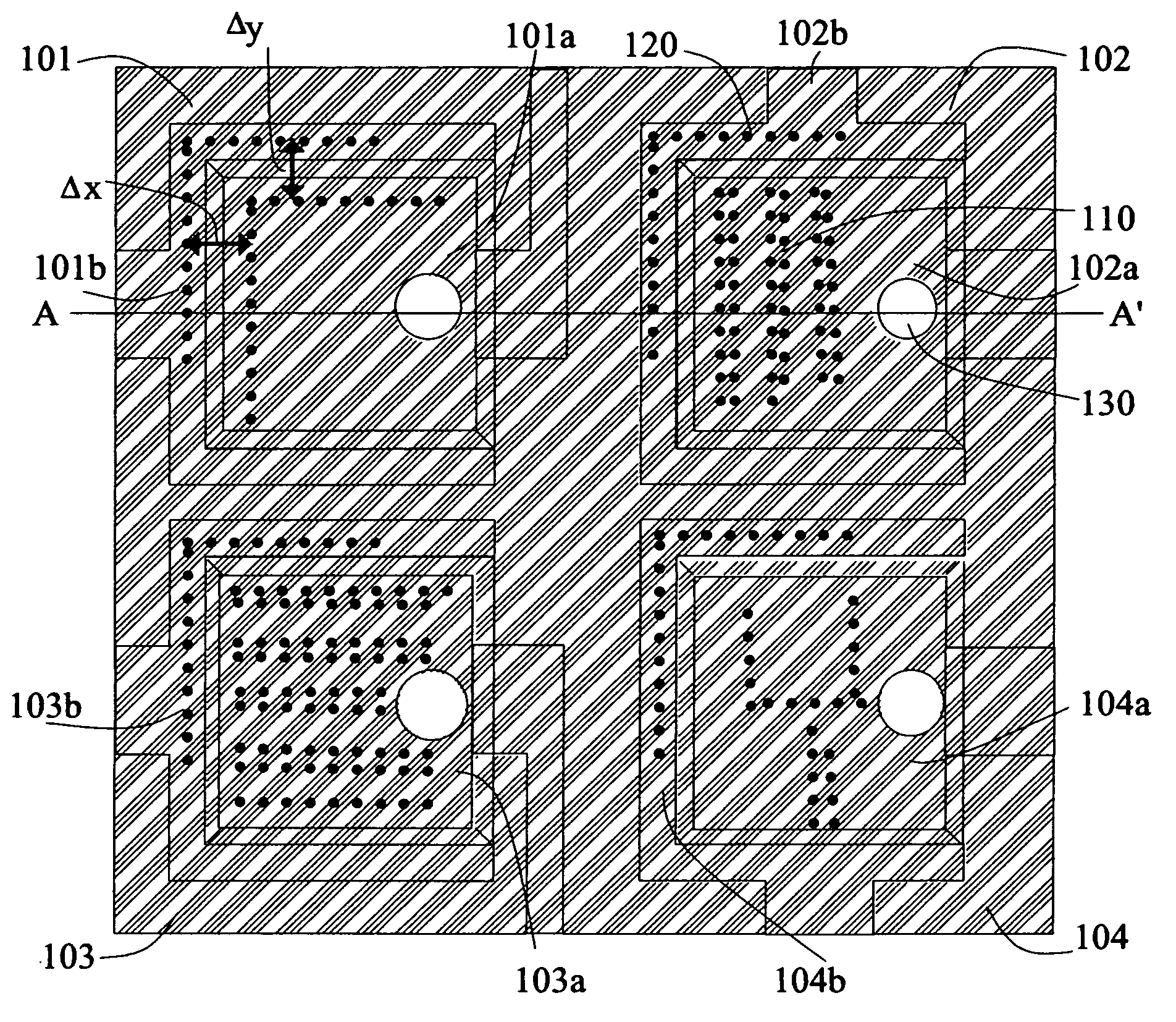
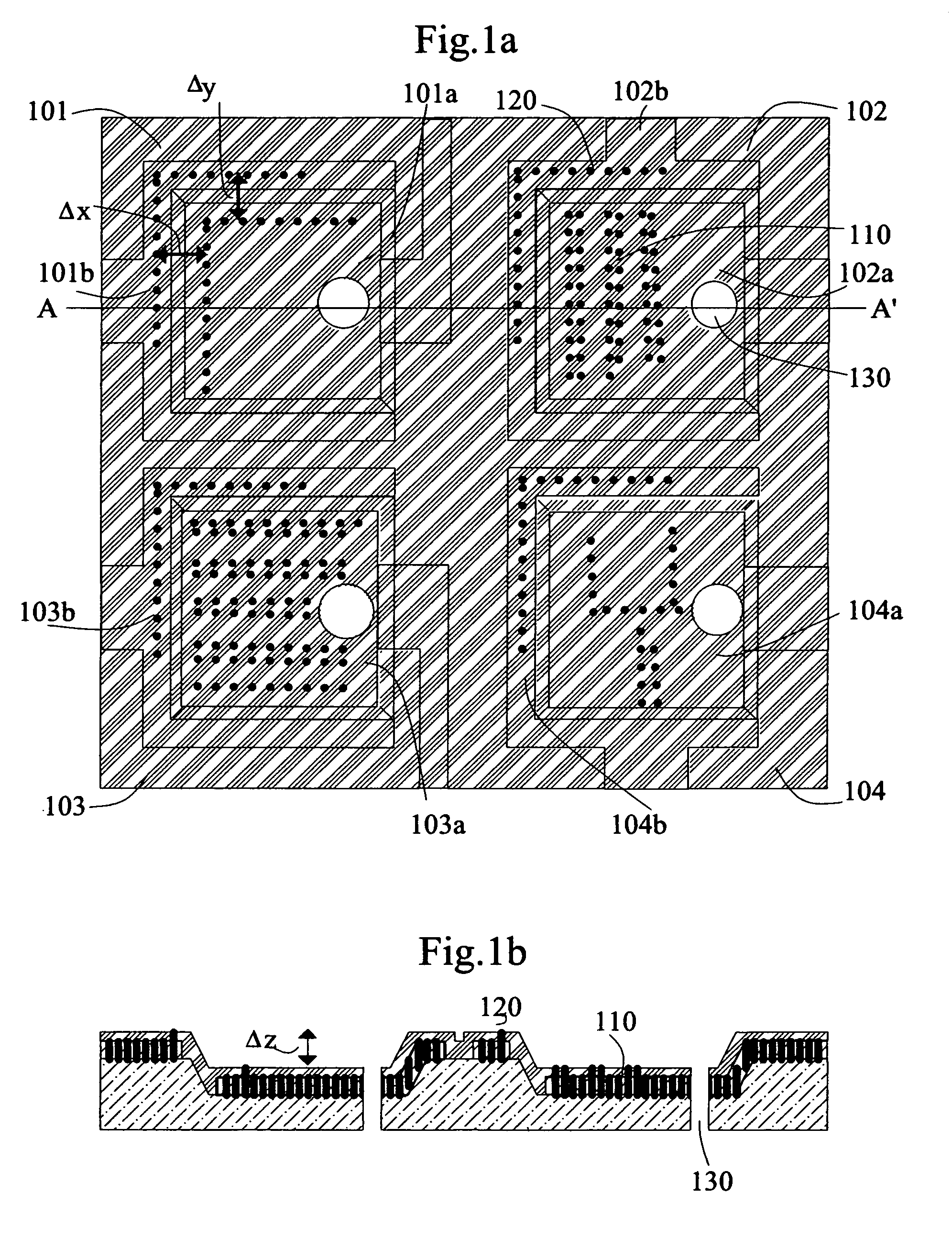
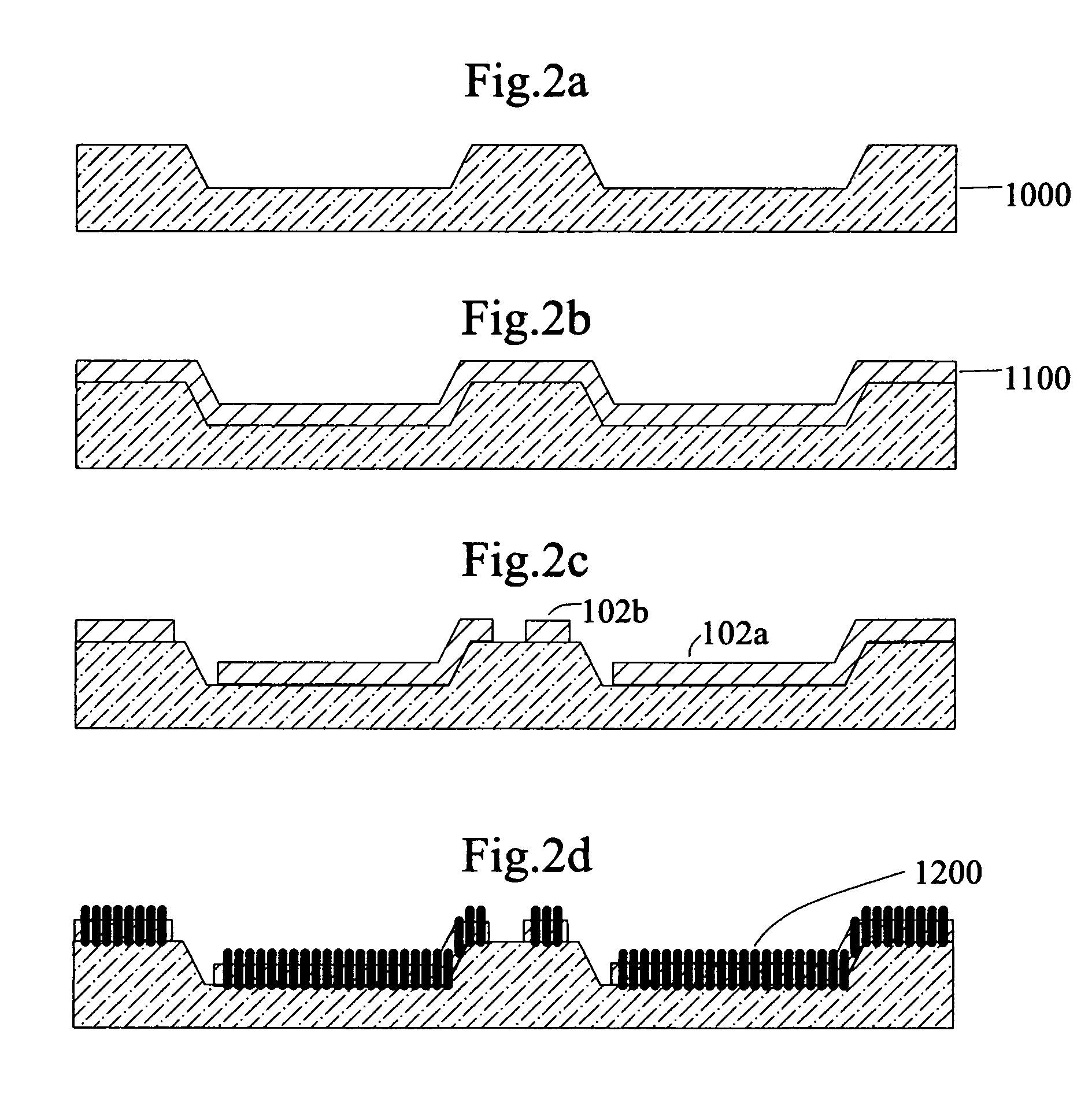
[0024]FIGS. 1a and 1b show the top and side view of one embodiment of the Parallel Electron Beam Lithography Stamp (PEBLS) system.

[0025]FIG. 1a illustrates four cells 101, 102, 103, 104, each of which include actuation electrodes 101a, 102a, 103a, 104a, with associated nanotip array patterns, and sensing electrodes 101b, 102b, 103b, 104b, with sensing nanotip patterns. Each cell size corresponds to the size of the area desired to be processed. For example, if the PEBLS is designed to pattern an area corresponding to microprocessor chip, cell sizes of 1 cm×1 cm may be appropriate. However, if the target of manufacture is a single circuit component such as an individual transistor, cell sizes in the micron range would be more appropriate. Multiple cells are provided each with an integrated alignment system 120 to achieve multiple process steps. However, if used for a single process step the alignment sensors 120 may be excl...


PUM


Abstract

An array of vertically aligned electron emitting nanotips such as multiwall carbon nanotubes are formed and patterned for use as a lithographic stamp. The spacing and / or arrangement of the nanotips correspond to a predetermined pattern that is desired to be formed on an opposing substrate. Simultaneous actuation of the nanotips by a common electrode forms a pattern on the opposing substrate without any necessary scanning techniques or use of masks. Applying a sufficient electrical potential between the array and the substrate generates electron emission from the tips so as to cure a resist, produce localized electrochemical reactions, establish localized electrostatic charge distributions or perform other desirable coating or etching process steps so as to create nanoelectronic circuitry or to facilitate molecular or nanoscale processing.

Description

FIELD OF THE INVENTION[0001]The present invention pertains to a tool and method used to form nanostructures or nano-structural features and is applicable to the fields of electronic fabrication, material processing, chemical processing, and biological processing at nanometer dimensions.BACKGROUND OF THE INVENTION[0002]Small scale fabrication has been dominated over the past 40 years by lithography techniques that employ radiation in the form or visible or ultraviolet light. However, these techniques are limited by the wavelengths of the light used and fabrication below 100 nm is problematic. Electron and ion beam lithography are alternative techniques capable of providing finer resolution but which typically use a serial scanning process that limits the speed of production.[0003]Two additional techniques that have received attention because of their ability to fabricate structures with nanometer resolutions are nanoimprint lithography and scanning probe lithography. These techniques...

Claims


Application Information

Patent Timeline
Patent Type & Authority Patents(United States)
IPC IPC(8): B05D1/04G01Q80/00
CPCB82Y10/00B82Y40/00G03F7/0002G03F7/2049H01J1/304H01J37/3177H01J2201/30469H01J2237/0635H01J2237/182H01J2237/2002Y10S977/953Y10S430/143Y10S977/947Y10S977/939
Inventor MOUTTET, BLAISE LAURENT
Owner MOUTTET BLAISE LAURENT
Why Eureka
Try Eureka