Improvements in external light efficiency of light emitting diodes

a technology light emitting diodes, which is applied in the direction of basic electric elements, semiconductor devices, electrical equipment, etc., can solve the problems of poor thermal conductivity, limited light extraction efficiency of conventional gan-based leds, and difficult to achieve further improvement, so as to improve the external light efficiency of light emitting diodes, reduce internal light reflection, and increase light output

a technology light emitting diodes, which is applied in the direction of basic electric elements, semiconductor devices, electrical equipment, etc., can solve the problems of poor thermal conductivity, limited light extraction efficiency of conventional gan-based leds, and difficult to achieve further improvement, so as to improve the external light efficiency of light emitting diodes, reduce internal light reflection, and increase light output

US20100295014A1Inactive Publication Date: 2010-11-25TINGGI TECH PTE

Image

  • Improvements in external light efficiency of light emitting diodes
  • Improvements in external light efficiency of light emitting diodes
  • Improvements in external light efficiency of light emitting diodes

Examples


Embodiment Construction

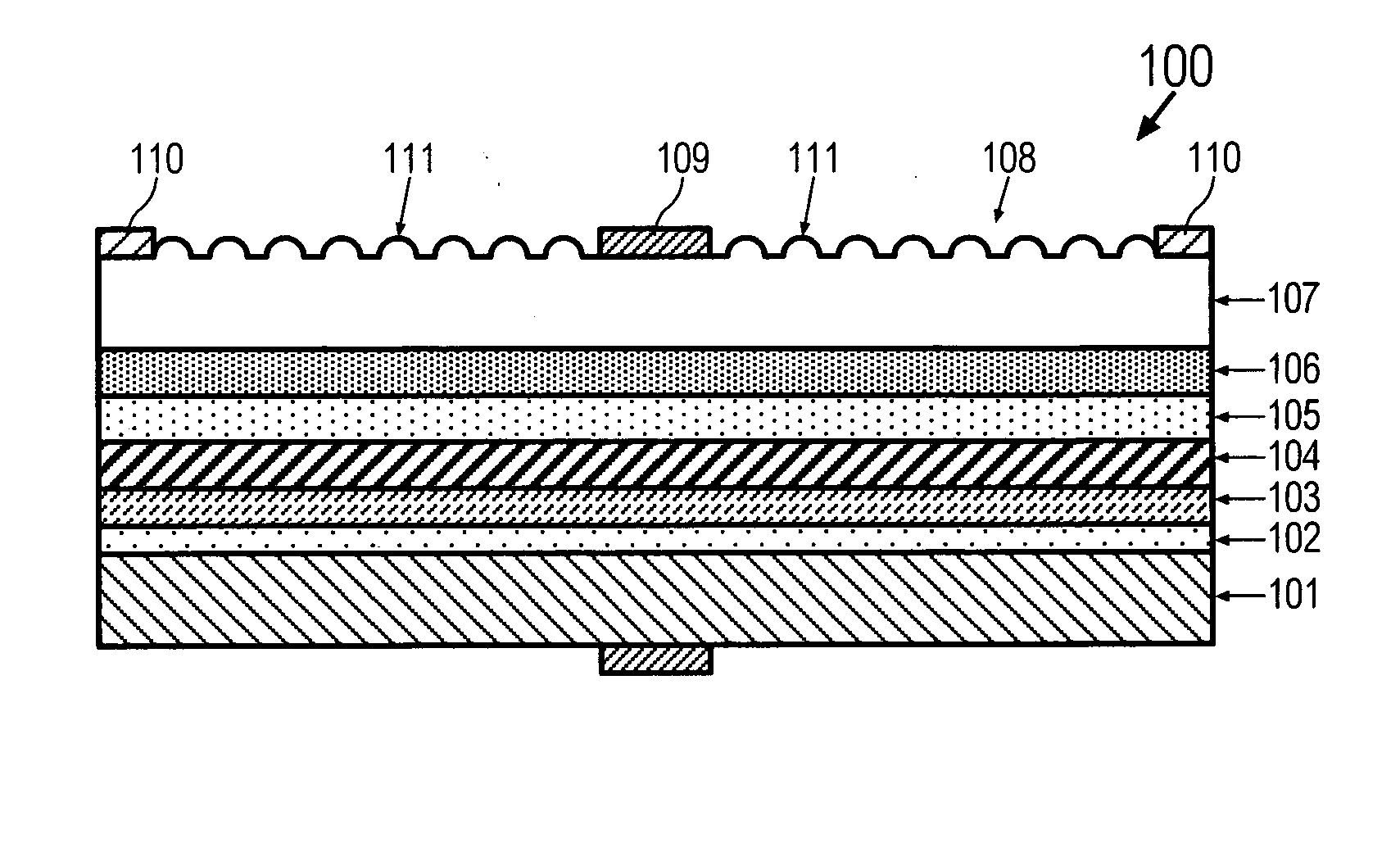
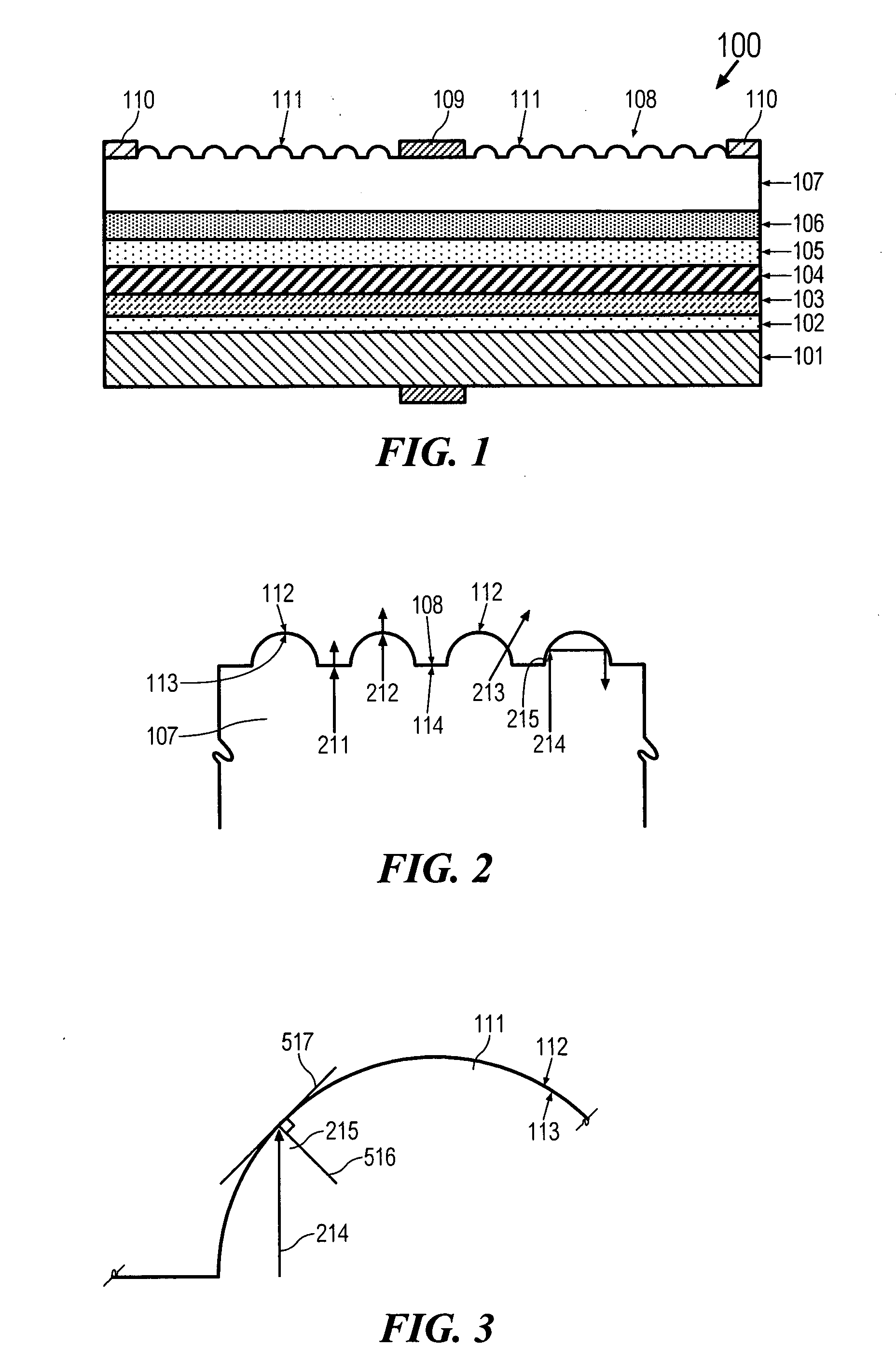
[0033]To refer to FIGS. 1 to 4 there is shown a first preferred embodiment being a light emitting diode 100 having:[0034]a first contact layer 101 of conductive metal;[0035]a seeding layer 102, a reflective layer 103;[0036]an ohmic contact layer 104;[0037]a p-type material layer 105 such as, for example, GaN;[0038]a plurality of epitaxial layers forming an active layer 106; and[0039]a conductive layer 107 of n-type material such as, for example, GaN.

[0040]Any layer may be a stack of multiple layers. The n-type layer 107 is relatively thick, whereas the p-type layer 105 is relatively thin. The active layer 106 may be one or more of: a quantum well, quantum wells, quantum dots and quantum wires.

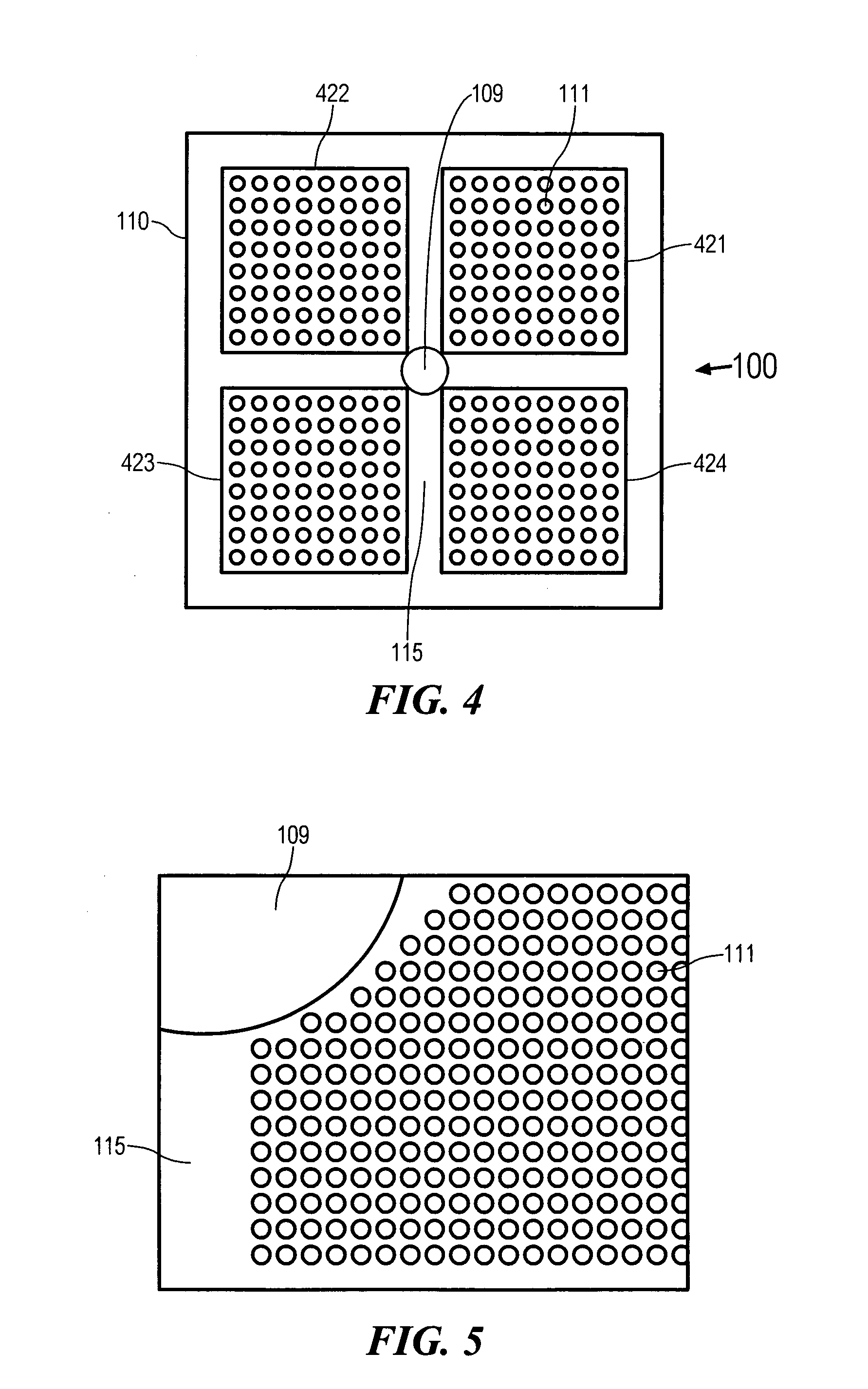
[0041]The conductive layer 107 is for the transmission of light generated in the active layer 106, the light passing through an external light output surface 108 of conductive layer 107. The external surface 108 is the external surface of the air-n-GaN interface. A bonding pad 109 is formed on ...


PUM


Abstract

A method to improve the external light efficiency of light emitting diodes, the method comprising etching an external surface of an n-type layer of the light emitting diode to form surface texturing, the surface texturing reducing internal light reflection to increase light output. A corresponding light emitting diode is also disclosed.

Description

FIELD OF THE INVENTION[0001]This invention relates to improvements in external light efficiency of light emitting diodes and refers particularly, though not exclusively, to light emitting diodes with surface texturing, include micro-lenses and / or surface roughening, on a light output surface, and a method of such surface texturing on a light output surface of light emitting diodes.BACKGROUND OF THE INVENTION[0002]Ga—N-based light emitting diodes (LEDs) have been intensively studied and developed in recent years. High efficiency, high power, GaN-based LEDs have attracted interest for applications such as displays, traffic signals, back lighting for mobile / cellular telephones and similar apparatus, and white light sources. Reducing cost and improving light output efficiency are important factors to enable such GaN LEDs to succeed in the mainstream lighting market.[0003]In general, the internal quantum efficiency (ηi) for GaN-based LEDs is significantly less than 100% due to crystal qu...

Claims


Application Information

Patent Timeline
25 Nov 2010
Publication
US20100295014A1
IPC
H01L33/04; H01L33/10; H01L33/30; H01L33/22; H01L33/40
CPC
H01L33/405; H01L33/22
Inventors
KANG, XUEJUN; CHEN, ZHEN