Connection structure between electrodes and touch panel

a technology of connecting structure and touch panel, which is applied in the direction of instruments, printed circuits, computing, etc., can solve the problems of poor adhesion performance and connection failur

Inactive Publication Date: 2010-11-25
OPTREX CORP
View PDF5 Cites 105 Cited by
  • Summary
  • Abstract
  • Description
  • Claims
  • Application Information

AI Technical Summary

Benefits of technology

[0019]In accordance with the present invention, it is possible to firmly connect two transparent electrodes disposed on a transparent substrate with another transparent electrode being placed therebetween.

Problems solved by technology

However, the inventors have found that the use of a resin for formation of the interlayer insulating film could cause a problem of poor adhesion performance for the ITO (Indium Tin Oxide) or the like, depending on the property of the used resin material, when each of the translucent electrode patterns or the relay electrode is formed of ITO (Indium Tin Oxide).
The inventors have found that such a connection structure could cause a problem in that when the electrode patterns 92 and 93, and the bridge wire 95 are made of ITO, and when the insulating film 94 is formed of a resin, the resin insulating film 94 peels at portions 98 and 99 riding on the electrode 92a and the electrode 92b since the resin insulating film 94 has a poor adhesion to ITO, with the result that the bridge wire 95 disposed as a top layer on the insulating film is lifted to cause a connection failure.

Method used


Image

  • Connection structure between electrodes and touch panel
  • Connection structure between electrodes and touch panel
  • Connection structure between electrodes and touch panel

Examples


Embodiment Construction

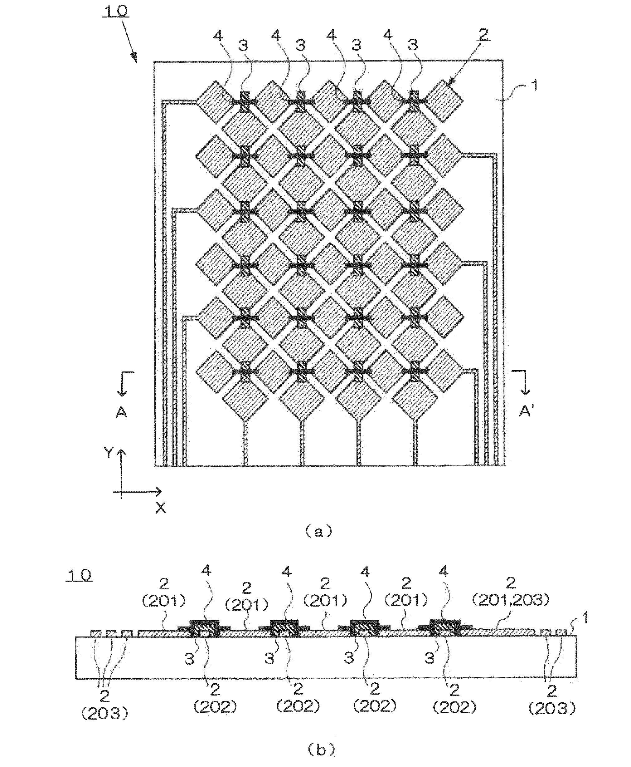
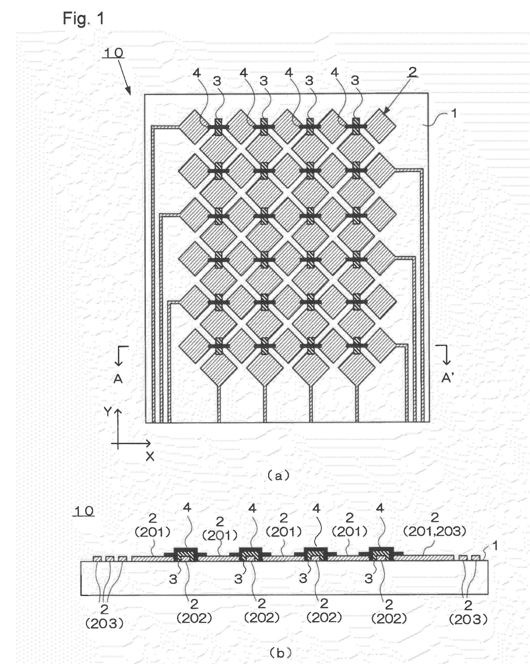
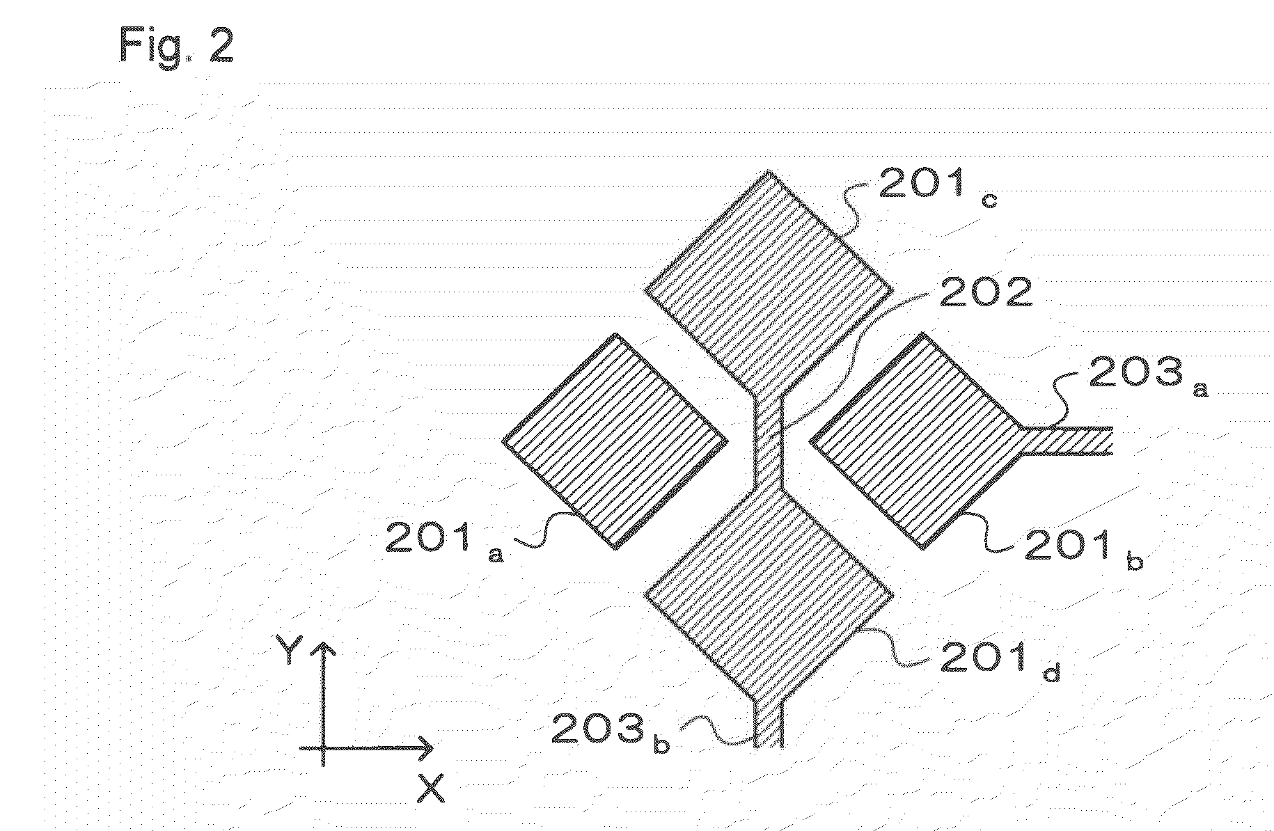
[0061]This example is a case where a touch panel has four electrode-array patterns for center electrodes and six electrode-array patterns for side electrodes in a matrix form in order to obtain a touch region having a width of 4 cm and a length of 6 cm. In this example, an ITO film was deposited so as to have a film thickness of 20 nm on a single side of a glass substrate having a thickness of 0.55 mm by a sputtering method and was patterned to form the respective electrode patterns 2 as shown in FIG. 3 by employing a photolithography technique. Specifically, the electrode elements 201 forming the respective electrode array patterns were set in a rhombus shape, and a transparent electrode pattern 2 was formed so as to include the six electrode-array patterns for the side electrodes 2-A1 to 2-A6 formed of groups of electrode elements aligned along the X-axis direction as a transverse direction, the four electrode-array patterns for the center electrodes 2-B1 to 2-B4 formed of groups ...


PUM


Abstract

A connection structure between electrodes includes a center electrode disposed as a transparent electrode on a transparent substrate; paired side electrodes disposed as transparent electrodes on the transparent substrate so as to place the center electrode therebetween; a bridge wire serving as a wire to connect between the paired side electrodes; and an electrically insulating film disposed between the center electrode and the bridge wire; wherein the bridge wire comprises a metal material; the electrically insulating film is disposed so as to be out of contact with the side electrodes at least within a certain range; and the bridge wire is disposed so as to be brought into direct contact with the transparent substrate in a gap region, the gap region being formed by disposing the electrically insulating film so as to bring out of contact with the side electrodes.

Description

BACKGROUND OF THE INVENTION[0001]1. Field of the Invention[0002]The present invention relates to a connection structure between electrodes for electrode connection on a substrate, and to a touch panel.[0003]2. Discussion of Background[0004]For example, there is a case where a first electrode pattern and a second electrode pattern are disposed to cross each other on a glass substrate forming a touch panel. With respect to the connection structure between electrodes in such a case, e.g. JP-A-2008-310550 discloses a capacitive input device, which includes a first translucent electrode pattern and a second translucent electrode pattern disposed on one side of a translucent substrate, wherein the second translucent electrode pattern, which is interrupted at portions where both patterns cross each other, is electrically connected by a relay electrode disposed on a top layer of an interlayer insulating film at each of the crossing portions (see paragraphs 0025 to 0027 and FIG. 8 of this re...

Claims


Application Information

Patent Timeline
Patent Type & Authority Applications(United States)
IPC IPC(8): G06F3/045H05K1/00
CPCG06F2203/04111G06F3/044G06F3/0443G06F3/0446
Inventor OZEKI, MASAOOTANI, SHINJUNISHIDA, SHUJI
Owner OPTREX CORP
Why Eureka
Try Eureka