Offset cancelling circuit

Inactive Publication Date: 2010-12-09
SEMICON COMPONENTS IND LLC
View PDF4 Cites 14 Cited by
  • Summary
  • Abstract
  • Description
  • Claims
  • Application Information

AI Technical Summary

Problems solved by technology

In the offset cancelling circuit 100 also due to the charge injection noise of the switching elements

Method used


Image

  • Offset cancelling circuit
  • Offset cancelling circuit
  • Offset cancelling circuit

Examples


Embodiment Construction

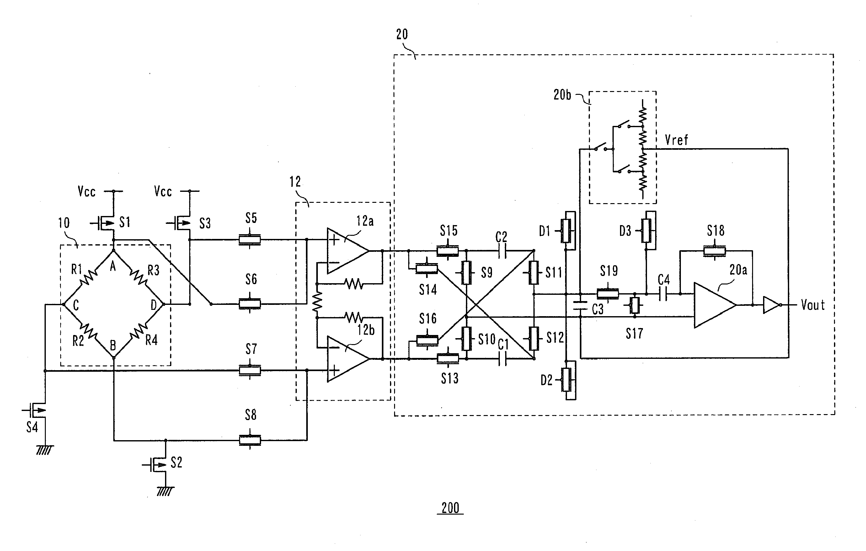
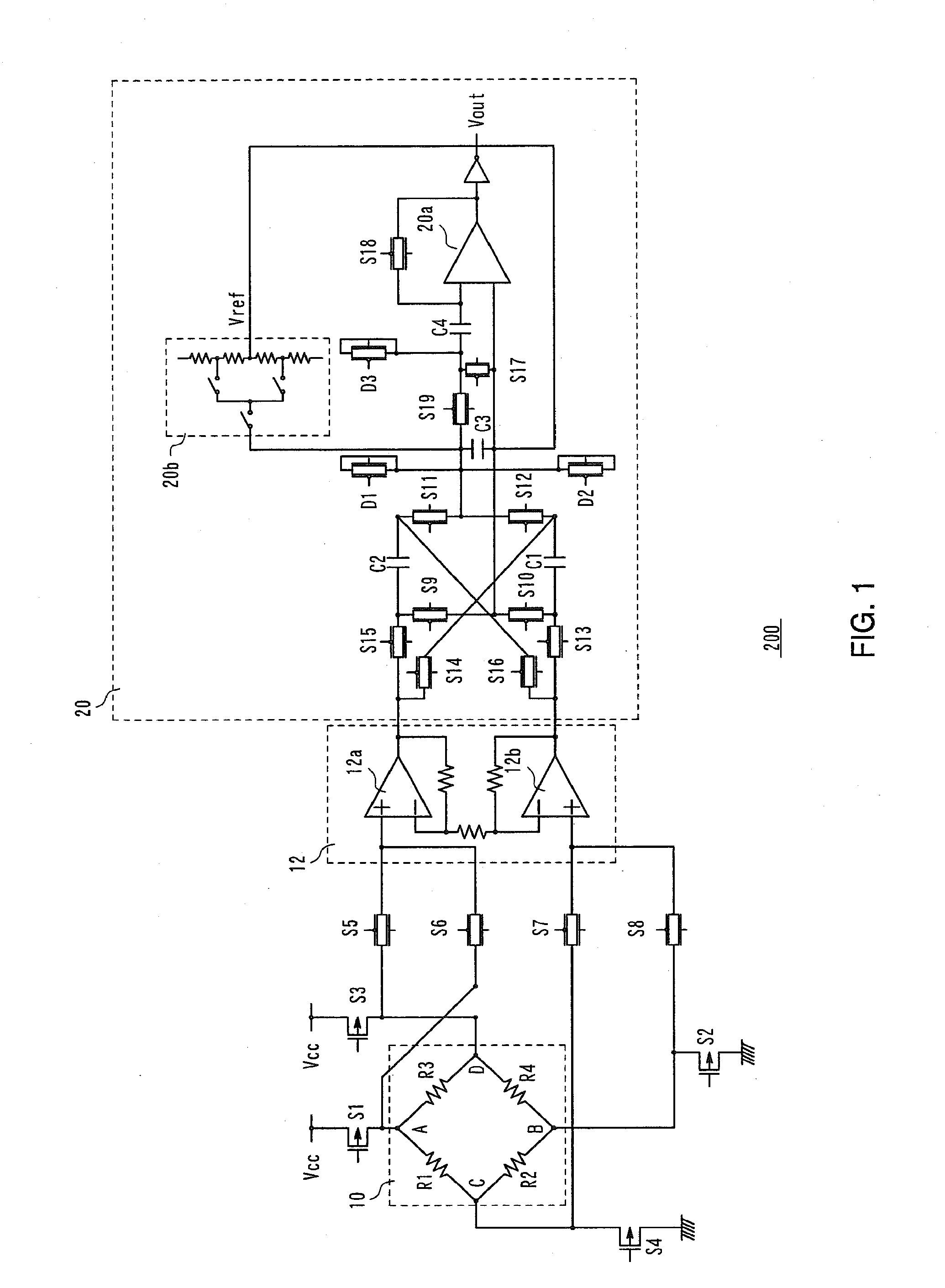
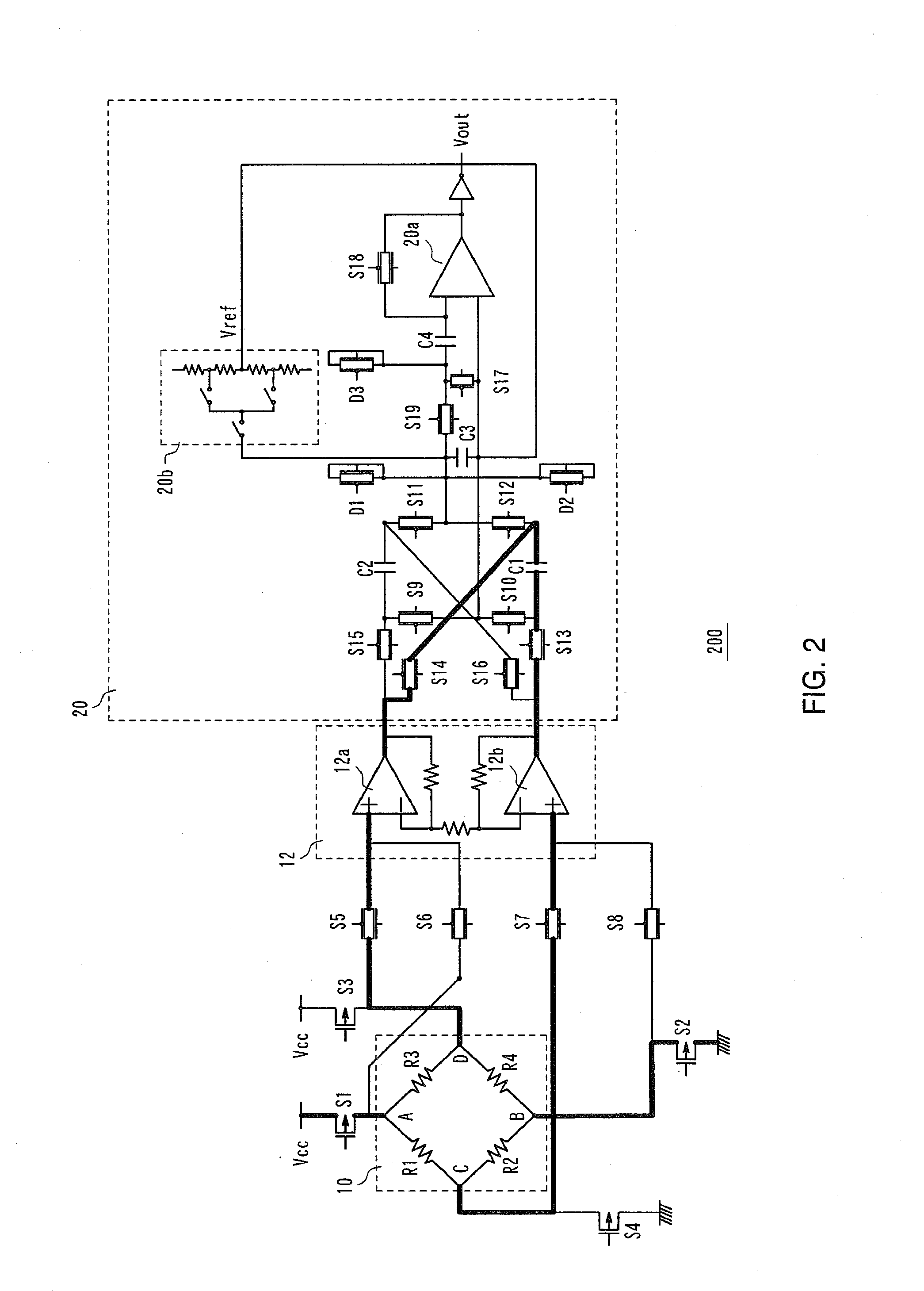
[0027]FIG. 1 shows a basic structure of an offset cancelling circuit 200 of a Hall element. The offset cancelling circuit 200 of the Hall element comprises a Hall element 10, an amplifier circuit 12, and an averaging circuit 20.

[0028]The Hall element 10 can be represented as a bridge circuit of resistors R1˜R4. Switching elements S1˜S8 which switch connection points A˜D of the resistors R1˜R4 to a power supply voltage Vcc, ground, or output are connected to the resistors R1˜R4.

[0029]The amplifier circuit 12 comprises operational amplifiers 12a and 12b. The operational amplifier 12a amplifies a voltage which is input to a non-inverting input terminal (+) and outputs the amplified voltage. The operational amplifier 12b amplifies a voltage which is input to a non-inverting input terminal (+) and outputs the amplified voltage.

[0030]The averaging circuit 20 comprises switching elements S9˜S19, dummy switching elements D1˜D3, capacitors C1˜C4, an operational amplifier 20a, and a reference...


PUM


Abstract

When a voltage is applied from outside such that a current flowing in a Hall element is switched, each of a plurality of capacitors is charged with an output voltage of the Hall element in each state. A dummy switching element is connected to a switching element which connects the plurality of capacitors in parallel to each other, the dummy switching element and the switching element being controlled to be switched ON and OFF exclusively with respect to each other.

Description

CROSS-REFERENCE TO RELATED APPLICATIONS[0001]The entire disclosure of Japanese Patent Application No. 2009-136906 filed on Jun. 8, 2009, including specification, claims, drawings, and abstract is incorporated herein by reference in its entirety.BACKGROUND[0002]1. Technical Field[0003]The present invention relates to an offset cancelling circuit which is used for adjustment of an output or the like of a Hall element.[0004]2. Related Art[0005]In recent years, image capturing devices such as a digital still camera and a digital video camera realize higher image quality by increasing the number of pixels of an image capturing element of the image capturing device. On the other hand, as another method for realizing higher image quality of the image capturing device, it is desired to equip the image capturing device with a vibration absorption control circuit having a shake correction function in order to prevent shaking of an imaging target caused by shaking of the hand holding the image...

Claims


Application Information

Patent Timeline
IPC IPC(8): H03L5/00H03F3/34
CPCG01R33/072H03K5/003H03F2203/45138H03F2200/261G01R33/07
Inventor OGAWA, TAKASHI
Owner SEMICON COMPONENTS IND LLC
Why Eureka
Try Eureka