
Thin film deposition apparatus

Inactive Publication Date: 2010-12-09
SAMSUNG DISPLAY CO LTD
View PDF99 Cites 40 Cited by
  • Summary
  • Abstract
  • Description
  • Claims
  • Application Information

AI Technical Summary

Benefits of technology

[0009]An aspect of the present invention provides a thin film deposition apparatus capable of forming a precise pattern on a large substrate.
[0041]According to an aspect of the present invention, the connection member may guide movement of the deposition material contained in the deposition source.
[0042]According to an aspect of the present invention, the connection member may seal a space among the deposition source, the first nozzle, and the second nozzle.

Problems solved by technology

However, it is difficult to achieve high light-emission efficiency with such a structure.
However, it is difficult to form fine patterns of organic thin films such as an organic emission layer or organic layers.
Thus, it is difficult to improve light emission characteristics of organic light-emitting display devices.
Also, recently, there is higher demand for large-sized display devices, but it is difficult to pattern organic thin films on a large surface using a conventional thin film deposition apparatus.
Thus, it is difficult to manufacture large-sized organic light-emitting display devices having satisfactory levels of driving voltage, current density, brightness, color purity, light emission efficiency, durability, etc.

Method used


Image

  • Thin film deposition apparatus
  • Thin film deposition apparatus
  • Thin film deposition apparatus

Examples


Embodiment Construction

[0074]Reference will now be made in detail to the present embodiments of the present invention, examples of which are illustrated in the accompanying drawings, wherein like reference numerals refer to the like elements throughout. The embodiments are described below in order to explain the present invention by referring to the figures. Moreover, it is to be understood that where is stated herein that one film or layer is “formed on” or “disposed on” a second layer or film, the first layer or film may be formed or disposed directly on the second layer or film or there may be intervening layers or films between the first layer or film and the second layer or film. Further, as used herein, the term “formed on” is used with the same meaning as “located on” or “disposed on” and is not meant to be limiting regarding any particular fabrication process

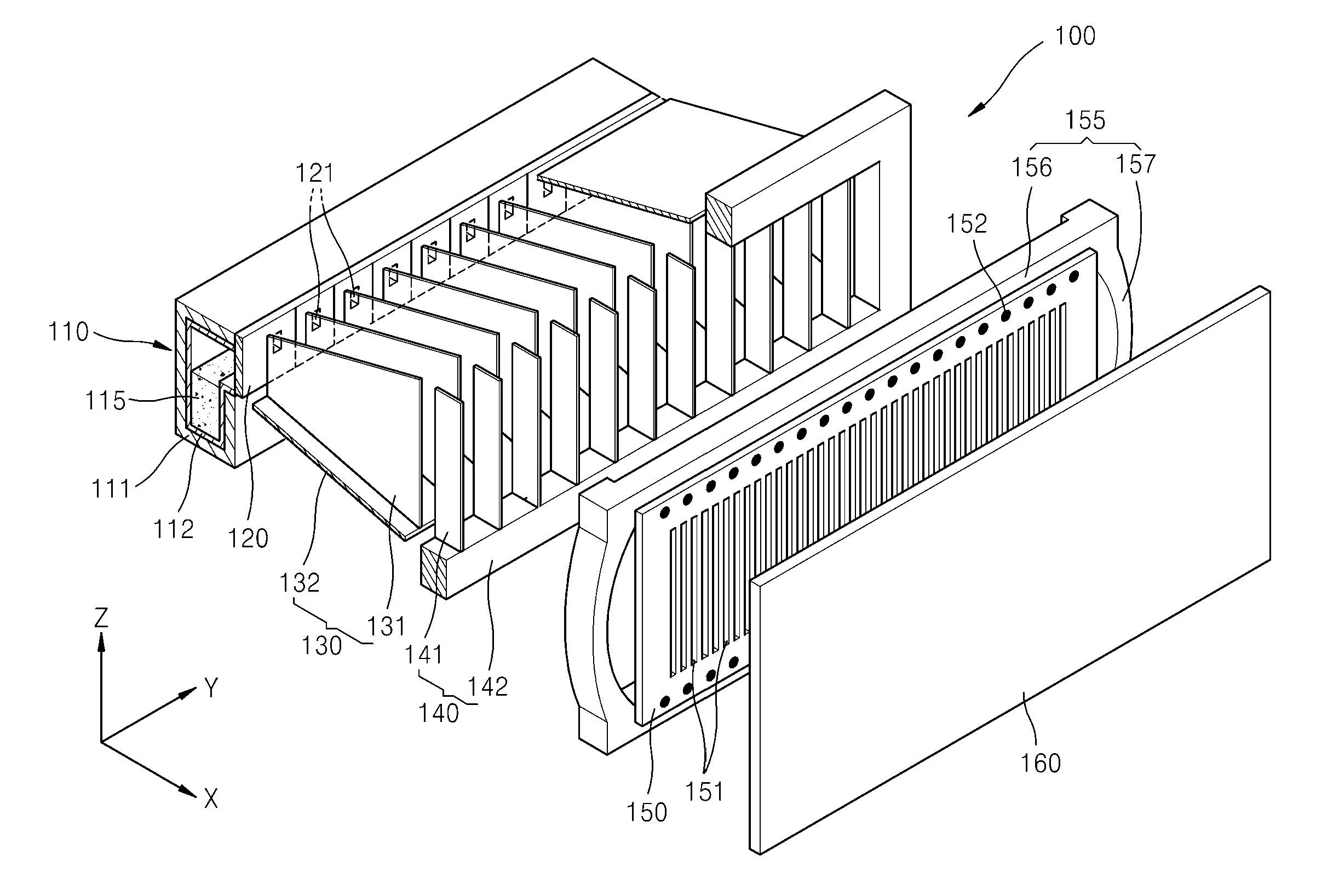
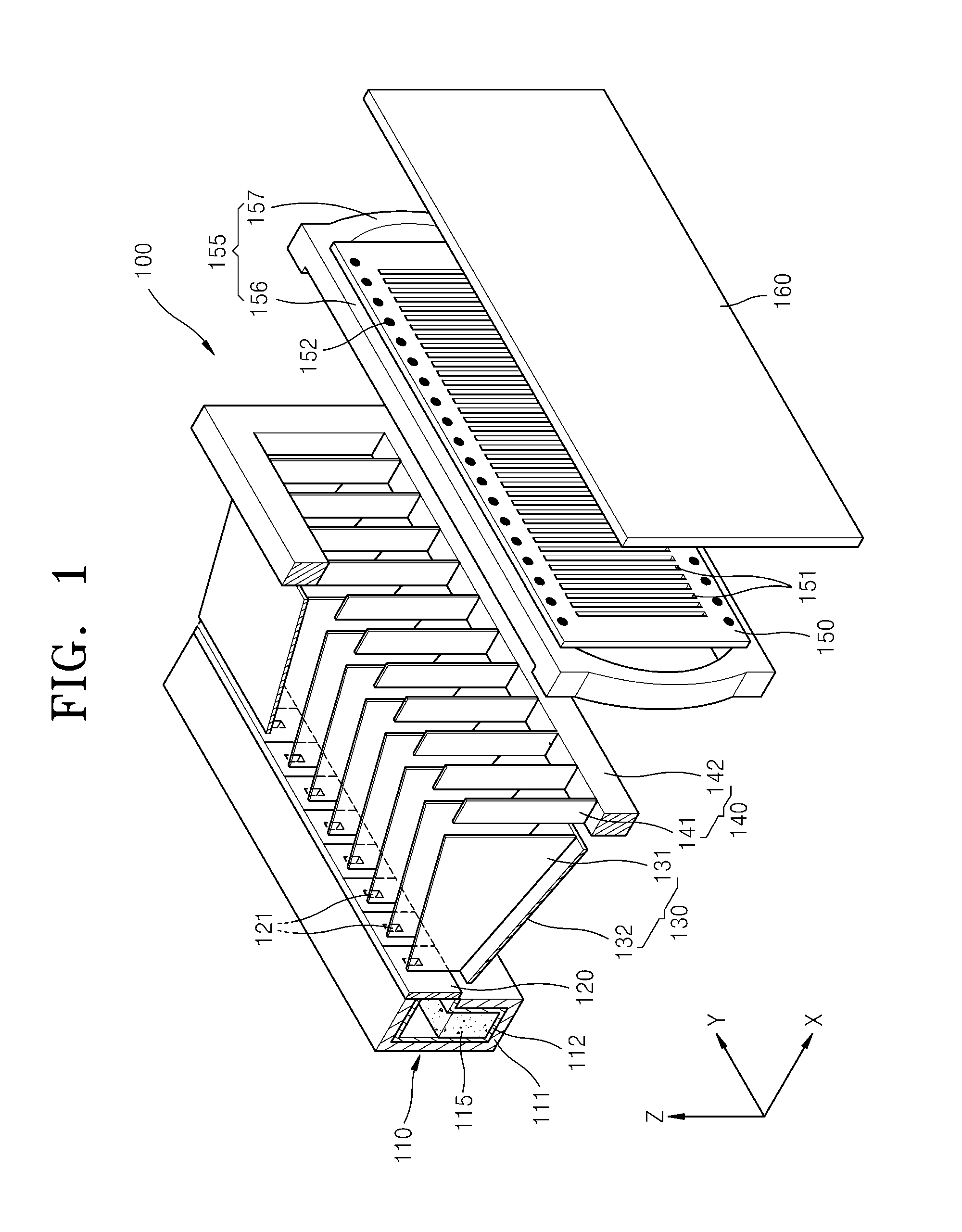
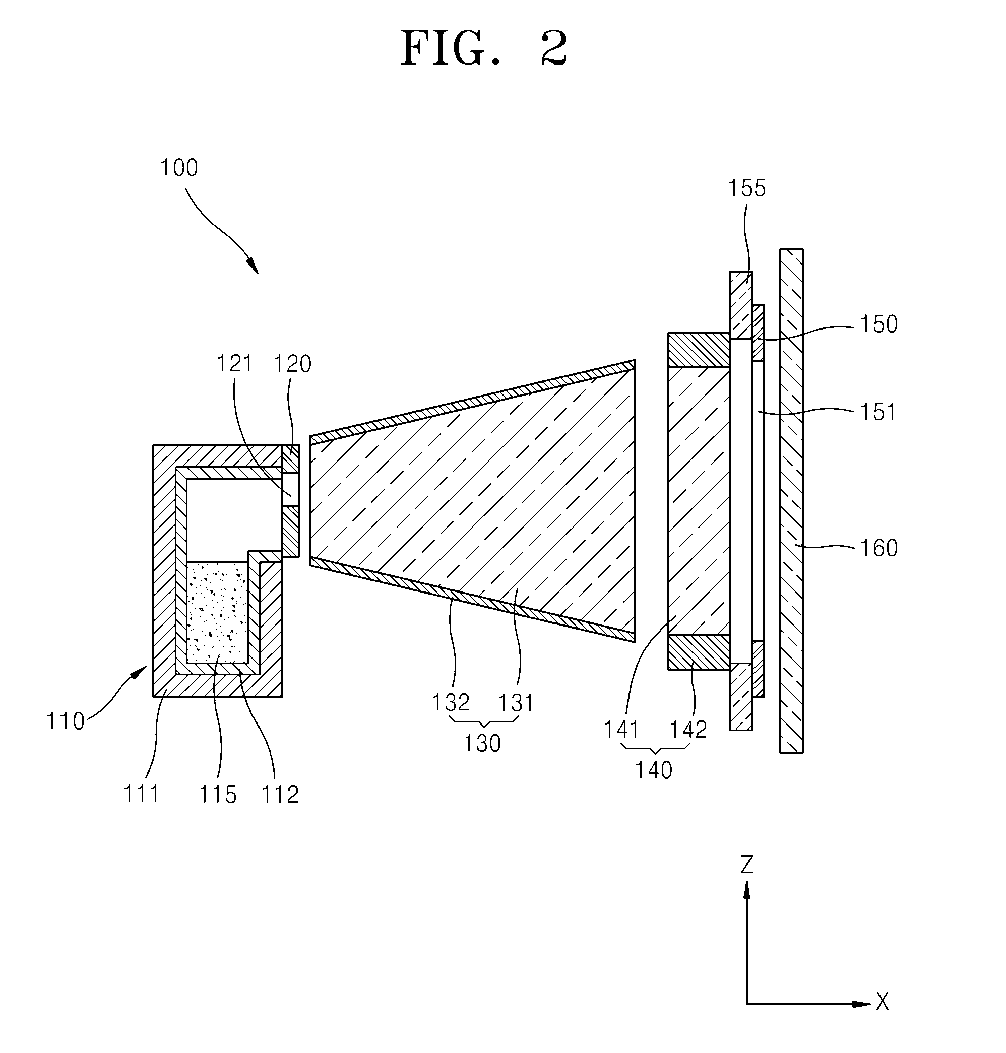
[0075]FIG. 1 is a schematic perspective view of a thin film deposition apparatus 100 according to an embodiment of the present invention. FIG...


PUM

PropertyMeasurementUnit
Timeaaaaaaaaaa
Lengthaaaaaaaaaa
Thicknessaaaaaaaaaa

Abstract

A thin film deposition apparatus capable of forming a precise deposition pattern on a large substrate includes a deposition source; a first nozzle disposed at a side of the deposition source having a plurality of first slits; a second nozzle disposed opposite to the first nozzle having a plurality of second slits; and a second nozzle frame bound to the second nozzle so as to support the second nozzle. The second nozzle frame includes two first frame portions spaced apart from each other and disposed in a direction in which the plurality of second slits are arranged, and two second frame portions each connecting the two first frame portions to each other, wherein the second frame portions are curved in the direction in which the plurality of second slits are arranged, so as to form arches.

Description

CROSS-REFERENCE TO RELATED APPLICATIONS[0001]This application claims the benefit of Korean Patent Application No. 10-2009-0050529, filed Jun. 8, 2009 and Korean Patent Application No. 10-2010-0010136, filed Feb. 3, 2010 in the Korean Intellectual Property Office, the disclosures of which are incorporated herein by reference.BACKGROUND[0002]1. Field[0003]Aspects of the present invention relate to a thin film deposition apparatus, and more particularly, to a thin film deposition apparatus capable of forming a precise pattern on a large substrate.[0004]2. Description of the Related Art[0005]Organic light-emitting display devices have a larger viewing angle, better contrast characteristics, and a faster response rate than other display devices, and thus have drawn attention as a next-generation display device. An organic light-emitting display device may generally generate visual light when holes and electrons respectively injected from an anode electrode and a cathode electrode are rec...

Claims


Application Information

Patent Timeline
IPC IPC(8): C23C16/455C23C16/00
CPCC23C14/243C23C14/044
Inventor LEE, CHOONG-HOLEE
Owner SAMSUNG DISPLAY CO LTD
Learn More