Fixed Jig, Chip Pickup Method and Chip Pickup Apparatus

a pickup method and chip technology, applied in the direction of machine supports, manufacturing tools, furniture parts, etc., can solve the problems of chip damage, chip may be broken, and the reliability of the semiconductor device in which the damaged chip is used is lower, so as to achieve safe transfer

Active Publication Date: 2010-12-16
LINTEC CORP
View PDF5 Cites 9 Cited by
  • Summary
  • Abstract
  • Description
  • Claims
  • Application Information

AI Technical Summary

Benefits of technology

[0016]A chip can be picked up in the following manner by the fixing jig in accordance with the present invention. A concave part formed on one side of the jig base is sectioned into small chambers by a partition. Consequently, when the contact layer on a small chamber is deformed by suctioning a through hole of the small chamber, a chip on the corresponding section can be detached from the contact layer. Thus the chip can be picked up.
[0017]By the chip pickup method and the chip pickup apparatus in accordance with the present invention, the chip can be picked up by only the suction force of the suction collet without the pushing up of the rear face of the chip using a fine needle. Consequently, the chip is not damaged.
[0018]Moreover, even for a chip that has been processed to be extremely thin, an individual chip can be reliably picked up and safely transferred to the next step.
[0019]Furthermore, by the chip pickup method and the chip pickup apparatus in accordance with the present invention, even in the case in which the suction collet picks up chips continuously, an adhesion state with a chip that remains on the fixing jig does not vary due to a leak of an air. Consequently, each chip can be fixed to the fixing jig with a stable small contact force at any time, therefore enabling each chip to be picked up without a displacement of the chip.

Problems solved by technology

Since a chip has been thinned, the pushing up of a chip by means of a fine needle delivers a considerable damage to the chip.
A semiconductor device in which a chip that has been damaged is used possesses lower reliability, for instance, a package crack occurs by receiving a heat history.
In addition, in the case in which a suffered damage is serious, a chip may be broken due to the pushing up of the chip in some cases.
However, in this method, a gap between chips cannot be sealed and an air leaks.
Moreover, a leak amount increases as a chip is picked up.

Method used


Image

  • Fixed Jig, Chip Pickup Method and Chip Pickup Apparatus
  • Fixed Jig, Chip Pickup Method and Chip Pickup Apparatus
  • Fixed Jig, Chip Pickup Method and Chip Pickup Apparatus

Examples


Embodiment Construction

[0040]An embodiment of the present invention will be described below in detail with reference to the drawings.

[0041]At first, a fixing jig that is used for the present invention will be described below.

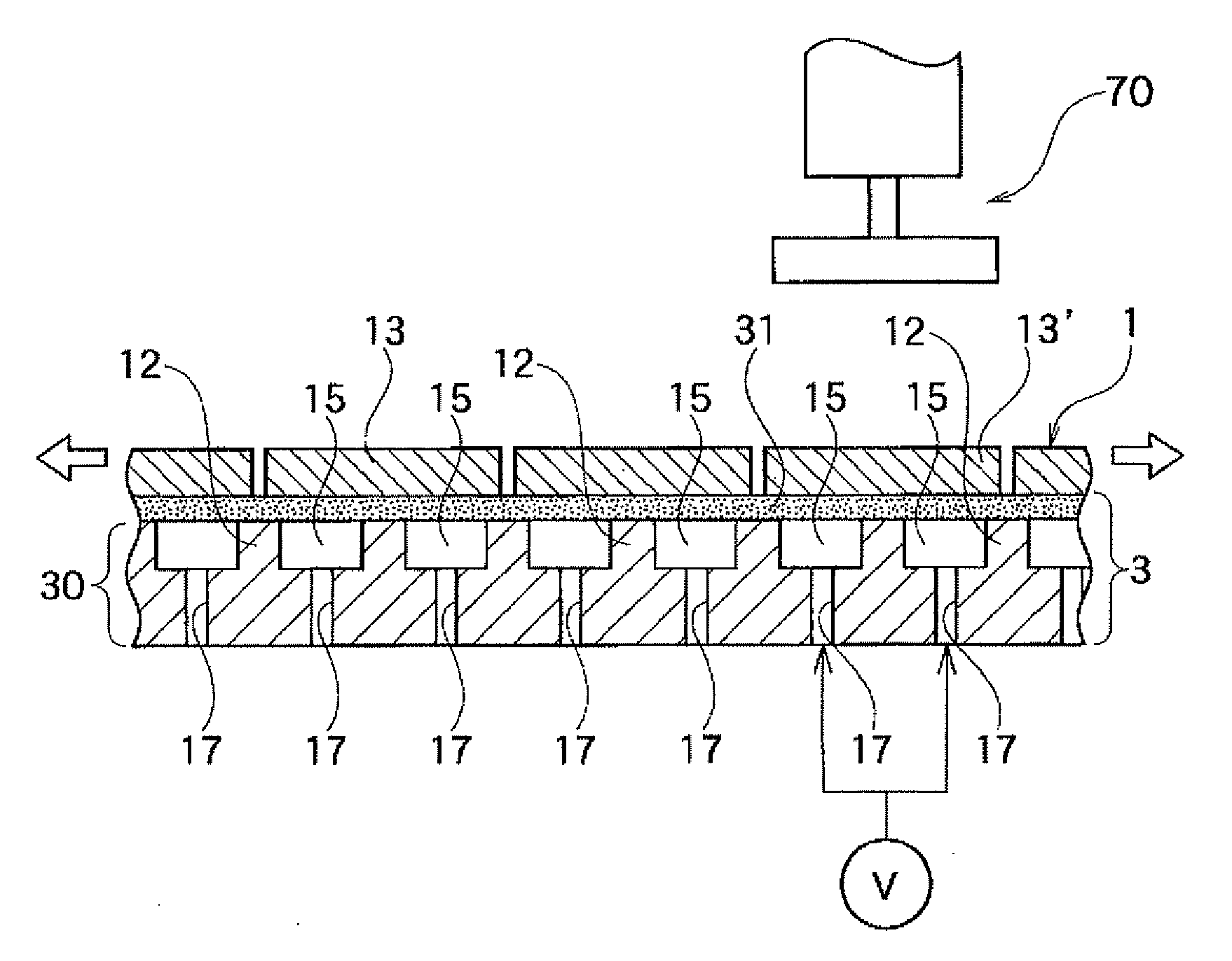
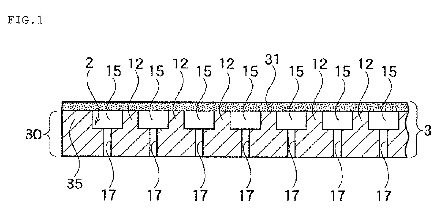
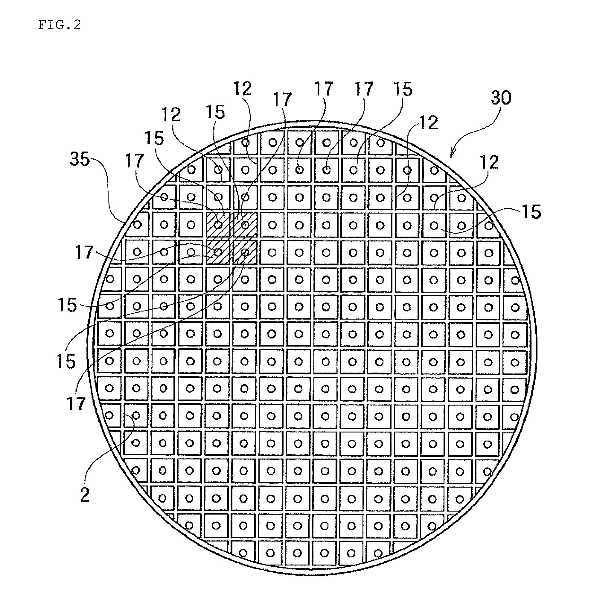
[0042]FIG. 1 shows a fixing jig in accordance with the present invention. The fixing jig is built in the pickup apparatus in accordance with the present invention to be used.

[0043]As shown in FIG. 1, a fixing jig 3 in accordance with the present invention is composed of a jig base 30 and an contact layer 31. As a shape of the jig base 30, there can be mentioned for instance an approximately circular shape, an approximately elliptical shape, an approximately rectangular shape, and an approximately polygonal shape, and an approximately circular shape as shown in FIG. 2 is preferable. A sidewall 35 is formed on the outer circumference section on one side of the jig base 30. A circular concave part 2 is formed inside the sidewall 35 on one side of the jig base 30. As shown in FIGS. 1 and ...


PUM

PropertyMeasurementUnit
thicknessaaaaaaaaaa
thicknessaaaaaaaaaa
diameteraaaaaaaaaa

Abstract

It is an object to provide a fixing jig which can unmovably suction a chip group produced by segmenting a semiconductor wafer into pieces, and can suction one chip by detaching the chip selectively and reliably from the chip group. A fixing jig 3 is composed of a jig base 30 and an contact layer 31. A concave part 2 is formed on one side of the jig base 30. The concave part 2 is sectioned into small chambers 15 by a partition 12 having a height almost equivalent to that of a sidewall 35. The contact layer 31 is disposed on the upper edge of the sidewall 35 and the partition 12 for covering the concave part 2. A through hole 17 that is communicated with the outside is formed in each small chamber 15.

Description

TECHNICAL FIELD[0001]The present invention relates to a fixing jig for fixing a chip group in a wafer shape produced by segmenting a semiconductor wafer into pieces, and a pickup method and a pickup apparatus in which the pushing up of a chip is not carried out. More specifically, the present invention relates to a fixing jig, a chip pickup method and a chip pickup apparatus in which a comparatively large-area semiconductor chip that has been ground to be extremely thin can be picked up individually without damage.BACKGROUND ART[0002]In recent years, an IC card and a mobile electronic device has been become popular and much further thinning of a semiconductor component has been desired. Consequently, a conventional semiconductor chip having a thickness of approximately 350 μm has to be further thinner to be in the range of 50 to 100 μm or less.[0003]To form a semiconductor chip, after a front surface circuit formation is carried out, a predetermined thickness of the semiconductor ch...

Claims


Application Information

Patent Timeline
Patent Type & Authority Applications(United States)
IPC IPC(8): H01L21/67B25J15/06B66C1/02F16M13/00H01L21/683
CPCH01L21/67132H01L21/6838Y10S156/941Y10T156/1168Y10T156/1944Y10T156/1978Y10T156/1132H01L21/52H01L21/67H01L21/683H01L21/78
Inventor WATANABE, KENICHISEGAWA, TAKESHIFUJIMOTO, HIRONOBU
Owner LINTEC CORP
Why Eureka
Try Eureka