Partitioned Replacement For Cache Memory
- Summary
- Abstract
- Description
- Claims
- Application Information
AI Technical Summary
Benefits of technology
Problems solved by technology
Method used
Image
Examples
Embodiment Construction
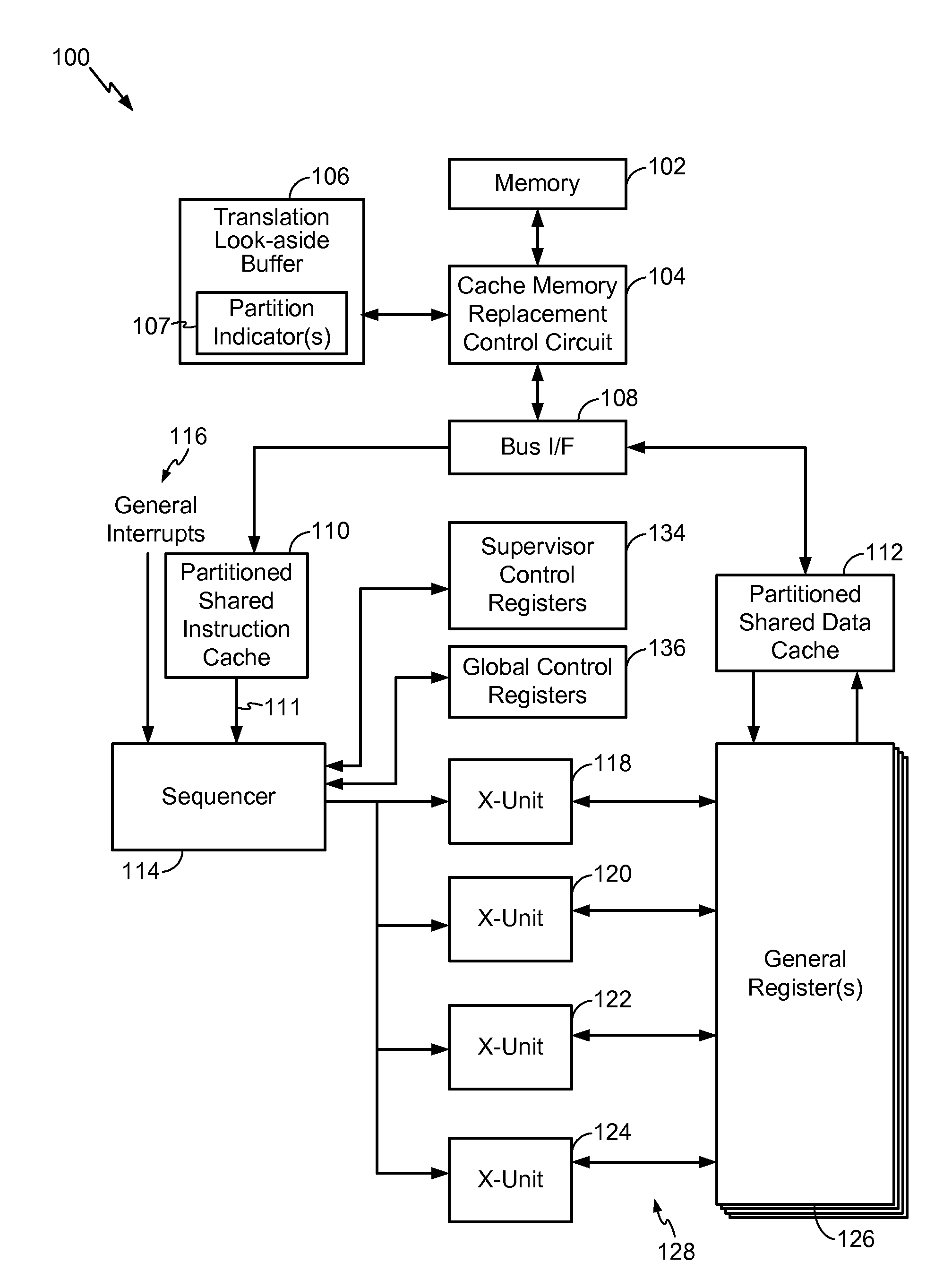
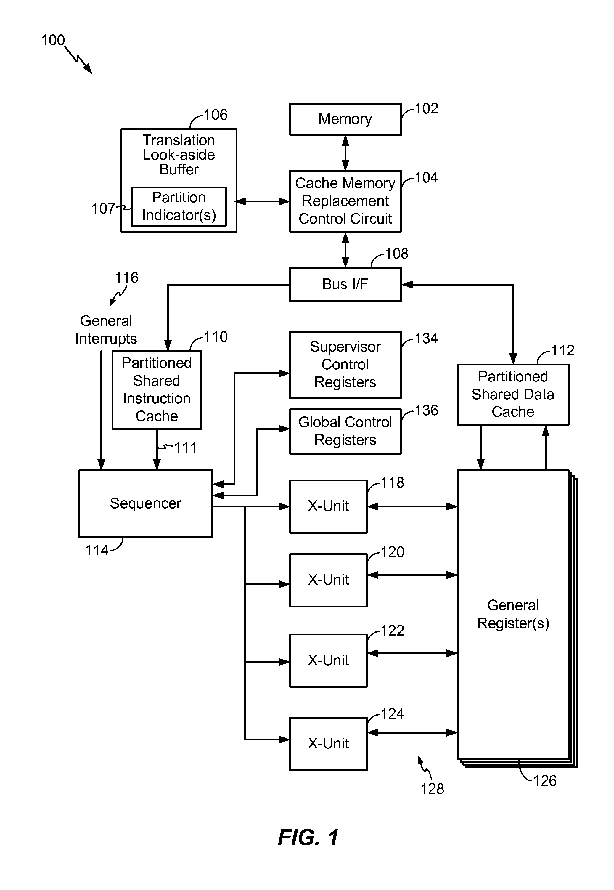
[0019]FIG. 1 is a block diagram of a particular illustrative embodiment of a processor 100 including a cache memory replacement control circuit 104 to manage cache replacement within a partitioned cache. In a particular example, the processor 100 may be a digital signal processor (DSP), a general-purpose processor, another type of processor, or any combination thereof. The processor 100 includes a memory 102 that is coupled to a partitioned shared instruction cache 110 and to a partitioned shared data cache 112 via a bus interface 108.
[0020]The cache memory replacement control circuit 104 is also coupled to the bus interface 108 and to a translation look-aside buffer (TLB) 106. The TLB 106 includes one or more table entries for translation of a virtual memory address to a physical memory address. Each table entry includes a partition identifier (i.e. partition bit or P-Bit) 107 identifying a partition of the partitioned shared instruction cache 110 or the partitioned shared data cac...
PUM
 Abstract
Description
Claims
Application Information


