Light emitting device and manufacturing method thereof

Active Publication Date: 2010-12-23
STANLEY ELECTRIC CO LTD
View PDF1 Cites 51 Cited by
  • Summary
  • Abstract
  • Description
  • Claims
  • Application Information

AI Technical Summary

Benefits of technology

[0016]With the light emitting device and the manufacturing method thereof according to the present invention, the reliabil

Problems solved by technology

This results in the bonding wire passing through the interface between the adhesive and encapsulating resin, and hence if the difference in thermal expansion coefficient between the adhesive and the encapsulating resin is large, the breaking of the bonding wire may happen due to a thermal shock, or so on, thus damaging reliability.
If peeling-off happens at the interface to the resin layer, in addition to the possibility of wire breaking, light may be reflected or scattered at the peeled-off portion, causing a problem in terms of light distribution design.
On the other hand, if the amount of adhesive is not enough, a space will be produced between the substrate and the reflector, so that air is likely to get confined between the reflector and the substrate when injecting resin.
Then, the air introduced under the reflector may intrude into the light emitting area t

Method used


Image

  • Light emitting device and manufacturing method thereof
  • Light emitting device and manufacturing method thereof
  • Light emitting device and manufacturing method thereof

Examples


first embodiment

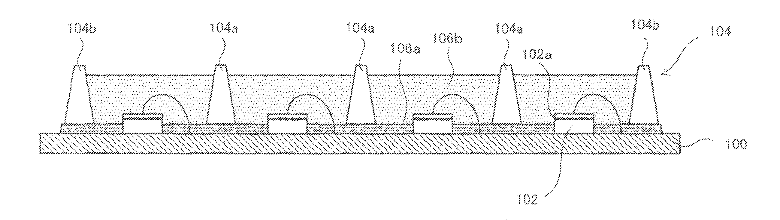
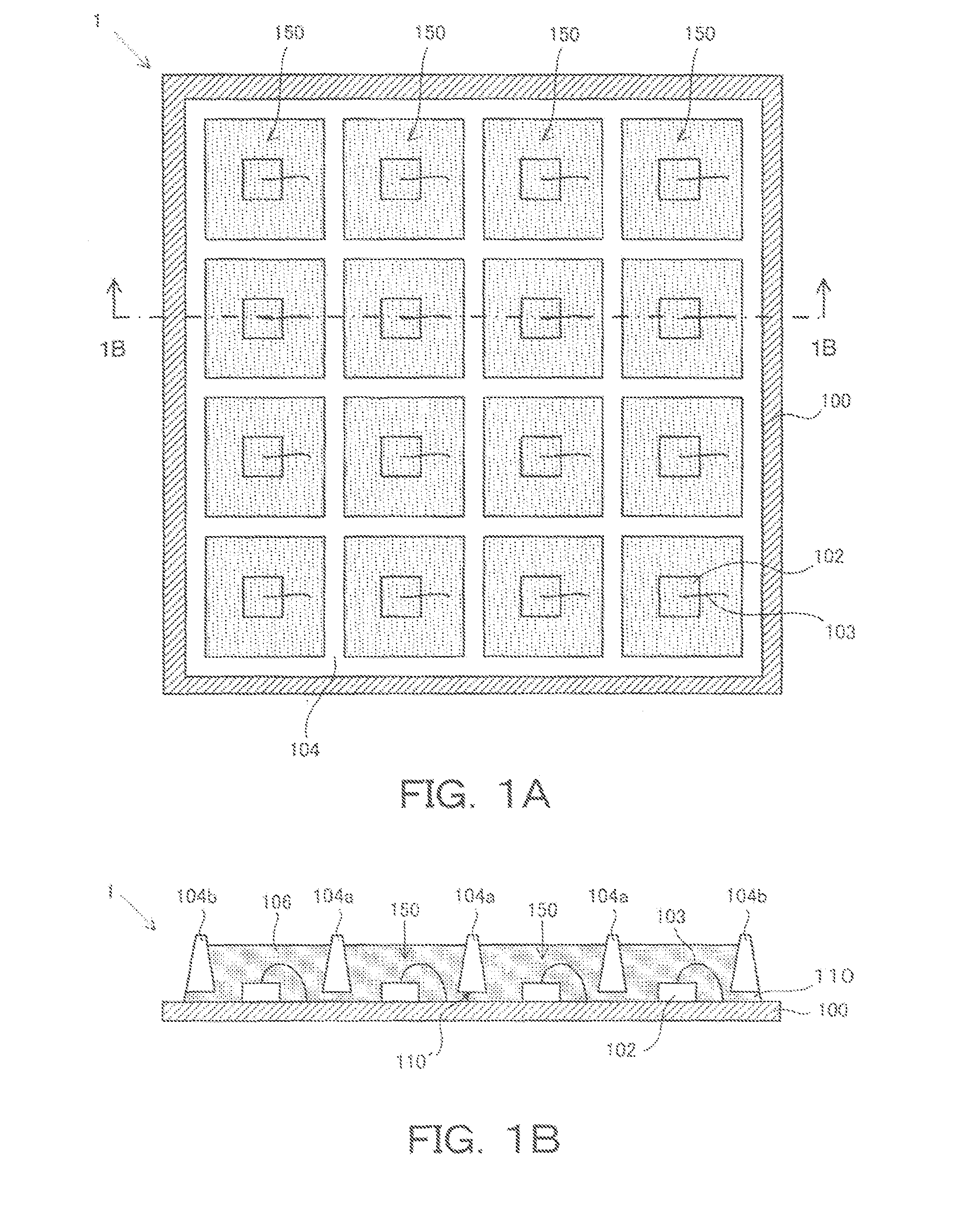
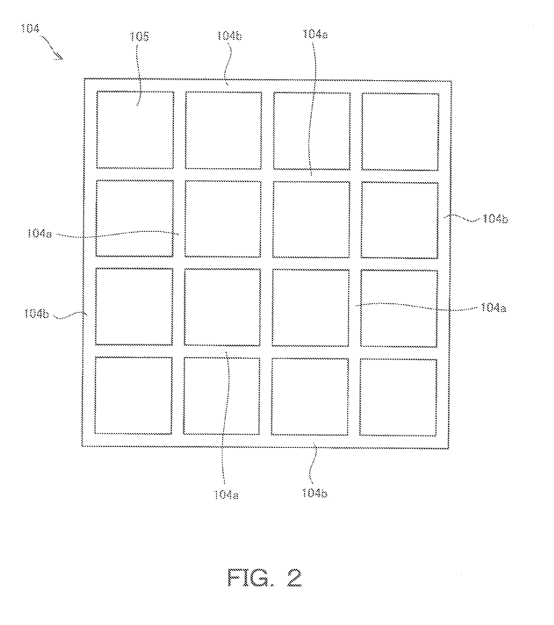
[0032]FIG. 1A is a top view showing the configuration of a light emitting device 1 according to a first embodiment of the present invention, and FIG. 1B is a cross-sectional view taken along line 1B-1B of FIG. 1A.

[0033]A substrate 100 is made of, e.g., glass epoxy resin or the like, and conductor lines (not shown) are formed on a surface of the substrate to feed power to a plurality of LED chips 102. For example, where the light emitting device 1 is used in application to a planar light source or a linear light source, a wiring pattern of conductor lines is formed to connect the LED chips 102 in series, in parallel, or in a combination of series and parallel. Note that the substrate 100 may be a metal substrate or a ceramic substrate instead of the resin substrate.

[0034]The plurality of LED chips 102 are fixed by a resin-based adhesive, solder, or the like at predetermined positions on the substrate 100. The LED chips 102 are arranged in rows and columns on the substrate 100. Each o...

second embodiment

[0055]FIG. 7 is a cross-sectional view showing the configuration of a light emitting device 2 according to a second embodiment of the present invention. In order to prevent resin leakage mentioned above, the light emitting device 2 differs from the light emitting device 1 according to the first embodiment in that the width d1 of the space 110b between the outer edge portion 104b of the reflector 104 and the substrate 100 is smaller than the width d2 of the spaces 110a between the partition wall portion 104a, i.e. the other portion than the outer edge portion 104b, of the reflector 104 and the substrate (d12). As such, by making the width of the space 110b located at the outermost circumference of the light emitting device 2 smaller than the width of the spaces 110a located on the inner circumference side, resin leakage can be prevented while obtaining the fluidity of the encapsulating resin 106 inward of the outer edge portion 104b. The widths d1 and d2 of the spaces should be set a...

third embodiment

[0056]FIG. 8 is a cross-sectional view showing the configuration of a light emitting device 3 according to a third embodiment of the present invention. In order to prevent resin leakage mentioned above, the light emitting device 3 differs from the light emitting device 1 according to the first embodiment in that the reflector 104 directly contacts the substrate 100 at the outer edge portion 104b, not via encapsulating resin. In other words, there is no space between the outer edge portion 104b of the reflector 104 and the substrate 100. The partition wall portion 104a, i.e. the other portion than the outer edge portion 104b, of the reflector 104 is apart from the substrate 100 as in the light emitting device 1 according to the first embodiment, and the space between them is filled with the encapsulating resin 106. With this configuration, resin leakage can be prevented while obtaining the fluidity of the encapsulating resin 106 inward of the outer edge portion 104b. Also, with this ...


PUM


Abstract

A light emitting device comprises a substrate having a plurality of light emitting elements mounted thereon; a side wall structure having a partition wall portion separating a plurality of light emitting areas that each include at least one of the light emitting elements; and encapsulating resin filled in the light emitting areas to bury the light emitting elements therein. The side wall structure is separated by a space from the substrate at, at least, the partition wall portion so as to be in noncontact with the substrate, and the encapsulating resin is formed so as to integrally, continuously fill the light emitting areas and the space without producing any interface therein.

Description

BACKGROUND OF THE INVENTION[0001]1. Field of the Invention[0002]The present invention relates to a light emitting device including a semiconductor light emitting element such as a light emitting diode (LED) and a manufacturing method thereof.[0003]2. Description of the Related Art[0004]Conventional examples of the configuration of a light emitting device, including a substrate having an LED chip mounted thereon and a reflector provided separately from the substrate, are as follows.[0005]Japanese Patent Application Laid-Open Publication No. H11-340517 discloses the configuration of a semiconductor light emitting device wherein a ring-shaped reflector is fixed onto a substrate to surround a semiconductor light emitting element, and wherein the reflector and the semiconductor light emitting element are buried with encapsulating resin.[0006]Japanese Patent Application Laid-Open Publication No. 2004-241509 discloses the configuration of an LED light source which includes a printed substr...

Claims


Application Information

Patent Timeline
IPC IPC(8): H01L33/52H01L21/56
CPCH01L25/0753F21Y2105/001H01L2224/48091H01L33/60F21Y2101/02H05K2203/1316H05K2203/049F21K9/90H05K3/284H05K2201/10106H05K2201/2054H01L2924/00014H01L2924/00F21Y2105/10F21Y2115/10
Inventor TACHIBANA, KAORI
Owner STANLEY ELECTRIC CO LTD
Why Eureka
Try Eureka