Liquid crystal display device and manufacturing method for same

a technology of liquid crystal display and manufacturing method, which is applied in the direction of microlithography exposure apparatus, semiconductor devices, instruments, etc., can solve the problems of small aperture ratio of pixels, abnormal alignment of proportions, and narrow surrounded signal lines

Active Publication Date: 2010-12-23
PANASONIC LIQUID CRYSTAL DISPLAY CO LTD
View PDF13 Cites 37 Cited by
  • Summary
  • Abstract
  • Description
  • Claims
  • Application Information

AI Technical Summary

Benefits of technology

[0015]Thus, the width of the overlapping portion of the color filters may be large in accordance with the small angle of the above described taper. In addition, the overlapping region of the color filters have a relatively large step, so that the alignment film formed on the surface that makes direct contact with the liquid crystal cannot be prevented from becoming abnormal in its alignment. Thus, portions with abnormal alignment are blocked from receiving light by making the width of the signal lines in the lower layer large, for example, and as a result, pixel regions surrounded by the signal lines become narrow, and the aperture ratio of the pixels becomes smaller.
[0016]An object of the present invention is to provide a liquid crystal display device with a higher aperture ratio.
[0018]Here, in a matrix of pixels, the color filters are red (R), blue (B) and green (G), for example, and color filters of the same color that cover pixels aligned in the direction y are aligned in such a manner that red (R), blue (B) and green (G) repeat in this order, for example, in the direction x. In this case, adjacent color filters of different colors overlap along the ends, and it is desirable for the width of the overlapping portion (amount of overlap of color) (color overlapping portion) and the height of the color overlapping portion (step of color overlap) to be small. This is because this makes the aperture ratio of the pixels is higher, the surface of the color filters flatter, and the alignment film more reliable.
[0054]In the above described Liquid crystal display device, it is possible to increase the aperture ratio. In addition, in the above described liquid crystal display device and according to the manufacturing method for the same, the angle of the taper in the contact holes is wider and the angle of the taper in the color overlapping portions is smaller in the COA color filter.

Problems solved by technology

In addition, the overlapping region of the color filters have a relatively large step, so that the alignment film formed on the surface that makes direct contact with the liquid crystal cannot be prevented from becoming abnormal in its alignment.
Thus, portions with abnormal alignment are blocked from receiving light by making the width of the signal lines in the lower layer large, for example, and as a result, pixel regions surrounded by the signal lines become narrow, and the aperture ratio of the pixels becomes smaller.

Method used


Image

  • Liquid crystal display device and manufacturing method for same
  • Liquid crystal display device and manufacturing method for same
  • Liquid crystal display device and manufacturing method for same

Examples


first embodiment

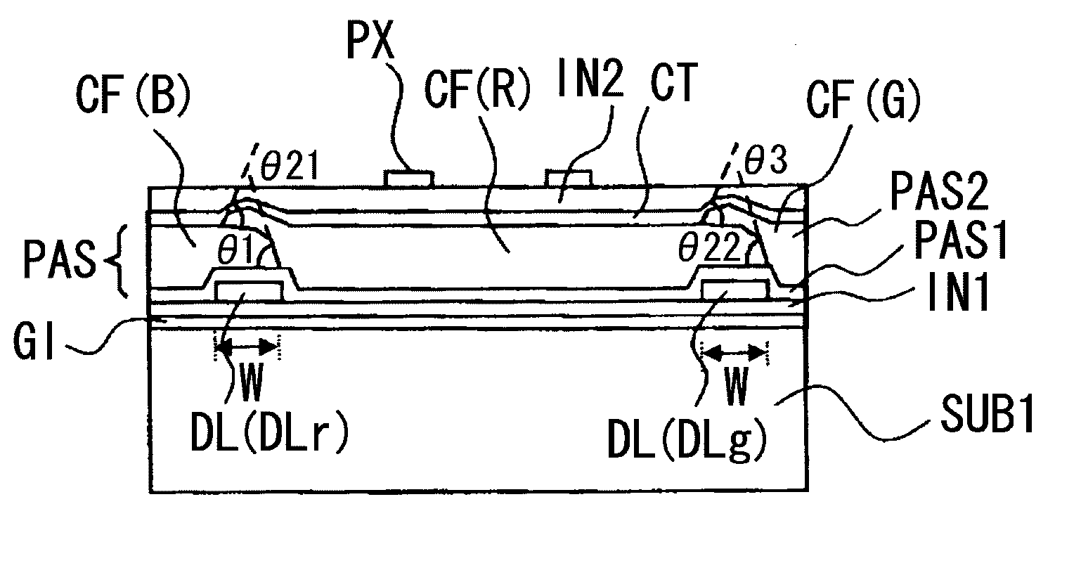
[0067]The liquid crystal display device according to the present invention has a pair of substrates that are positioned so as to face each other and sandwich liquid crystal, wherein gate signal lines made of a light blocking material which run in a first direction and are aligned in a second direction which crosses the above described first direction, and drain signal lines made of alight blocking material which run in the above described second direction and are aligned in the above described first direction, are formed on the surface of one of the two substrates, on the liquid crystal side, and thin film transistors which are turned on by a scanning signal through a gate signal line and pixel electrodes to which a video signal is supplied from a drain signal line through a thin film transistor when turned on are provided in pixel regions, pixel regions being defined as regions surrounded by two adjacent gate signal lines and two adjacent drain signal lines. Furthermore, each of th...

second embodiment

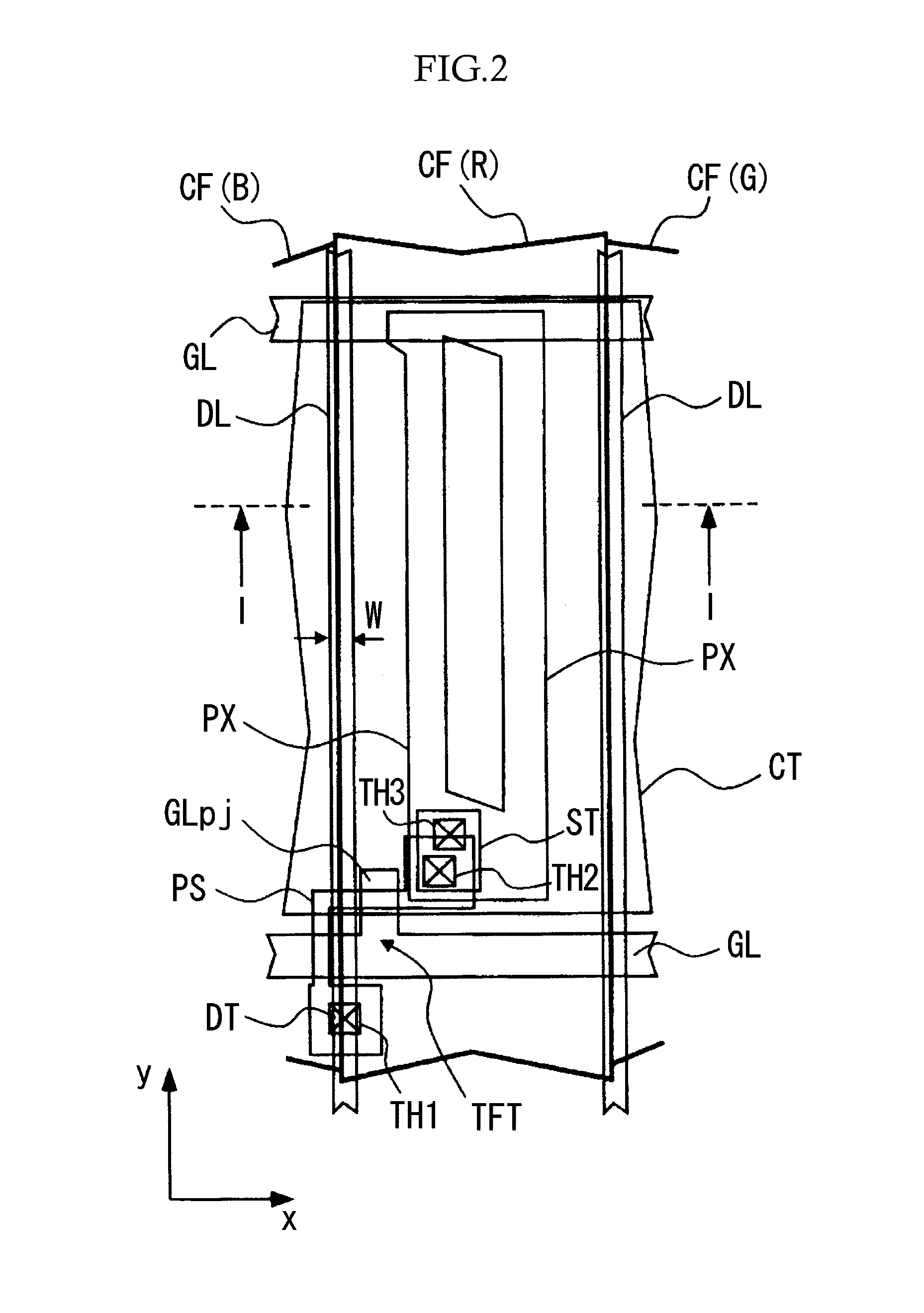
[0092]The second embodiment onward have more or less the structure shown in FIGS. 1 to 3, and therefore, the following descriptions are also based on Table 1.

[0093]The product for which the invention is used is the same as in the first embodiment. The order in which color filters CF for each pixel are layered in unit pixels is green (G), red (R) and blue (B). In the following descriptions, green is simply referred to as G, red is simply referred to as R, and blue is simply referred to as B for the sake of simplicity.

[0094]The density of the pigment in the color filters G is 20%, the film thickness is 4.0 μm, the relative dielectric constant is 3.6, and the angle of the taper is 45°. The density of the pigment in the color filters R is 10%, the film thickness is 4.0 μm, the relative dielectric constant is 3.0, and the angle of the taper is 45°. The density of the pigment in the color filters B is 10%, the film thickness is 4.0 μm, the relative dielectric constant is 3.3, and the angl...

third embodiment

[0095]The product for which the invention is used is the same as in the first embodiment. The order in which color filters for each pixel are layered in unit pixels is B, R and G.

[0096]The density of the pigment in the color filters B is 40%, the film thickness is 1.0 μm, the relative dielectric constant is 5.0, and the angle of the taper is 70°. The density of the pigment in the color filters R is 50%, the film thickness is 1.0 μm, the relative dielectric constant is 6.0, and the angle of the taper is 80°. The density of the pigment in the color filters G is 60%, the film thickness is 1.0 μm, the relative dielectric constant is 7.0, and the angle of the taper is 90°. The difference in thickness between the color filters for B and the color filters for R overlapping the color filters for B is 0.4 μm, the difference in thickness between the color filters for B and the color filters for G overlapping the color filters for B is 0.6 μm, and the difference in thickness between the color ...


PUM

PropertyMeasurementUnit
widthaaaaaaaaaa
widthaaaaaaaaaa
angleaaaaaaaaaa

Abstract

A liquid crystal display device with a higher aperture ratio is provided. According to one embodiment of the present invention, second color filters are formed so as to overlap with first color filters when adjacent color filters having different colors are formed on the TFT substrate side, so that the angle of the first tapers where said first color filters overlap and the angle of the second tapers where said second color filters overlap are set to 45° or more and 90° or less.

Description

CROSS-REFERENCE TO RELATED APPLICATION[0001]The present application claims priority over Japanese Applications JP2009-145057 filed on Jun. 18, 2009 and JP2009-220215 filed on Sep. 25, 2009, the contents of which are hereby incorporated into this application by reference.BACKGROUND OF THE INVENTION[0002](1) Field of the Invention[0003]The present invention relates to a liquid crystal display device and a manufacturing method for the same, and in particular, to a so-called COA (color-filter on array) liquid crystal display device where color filters are provided on the TFT substrate side, as well as a manufacturing method for the same.[0004](2) Description of the Related Art[0005]Liquid crystal display devices (panels) have a pair of substrates that are positioned so as to face each other and sandwich liquid crystal as a housing, and thus are formed so that the light transmittance of the liquid crystal can be independently controlled in each pixel. Therefore, a number of pixels, which...

Claims


Application Information

Patent Timeline
Patent Type & Authority Applications(United States)
IPC IPC(8): G09G3/36G03F7/20G02F1/1335
CPCG02F1/136227G02F2001/136236G02F2001/136222G02F1/136236G02F1/136222G02F1/133514G02F1/134309G02F1/136209G02F1/136286G02F1/1368H01L27/1214H01L27/1222H01L27/124H01L29/78675
Inventor MIZUNO, YASUHIROTANNO, JUNJIHAYAHARA, SHINSUKESAKURAI, MASATOKIMURA, YASUKAZUFUJIYOSHI, JUN
Owner PANASONIC LIQUID CRYSTAL DISPLAY CO LTD
Why Eureka
Try Eureka