
Thermoelectric element and thermoelectric device
- Summary
- Abstract
- Description
- Claims
- Application Information
AI Technical Summary
Benefits of technology
Problems solved by technology
Method used
Image

Examples
embodiment 1
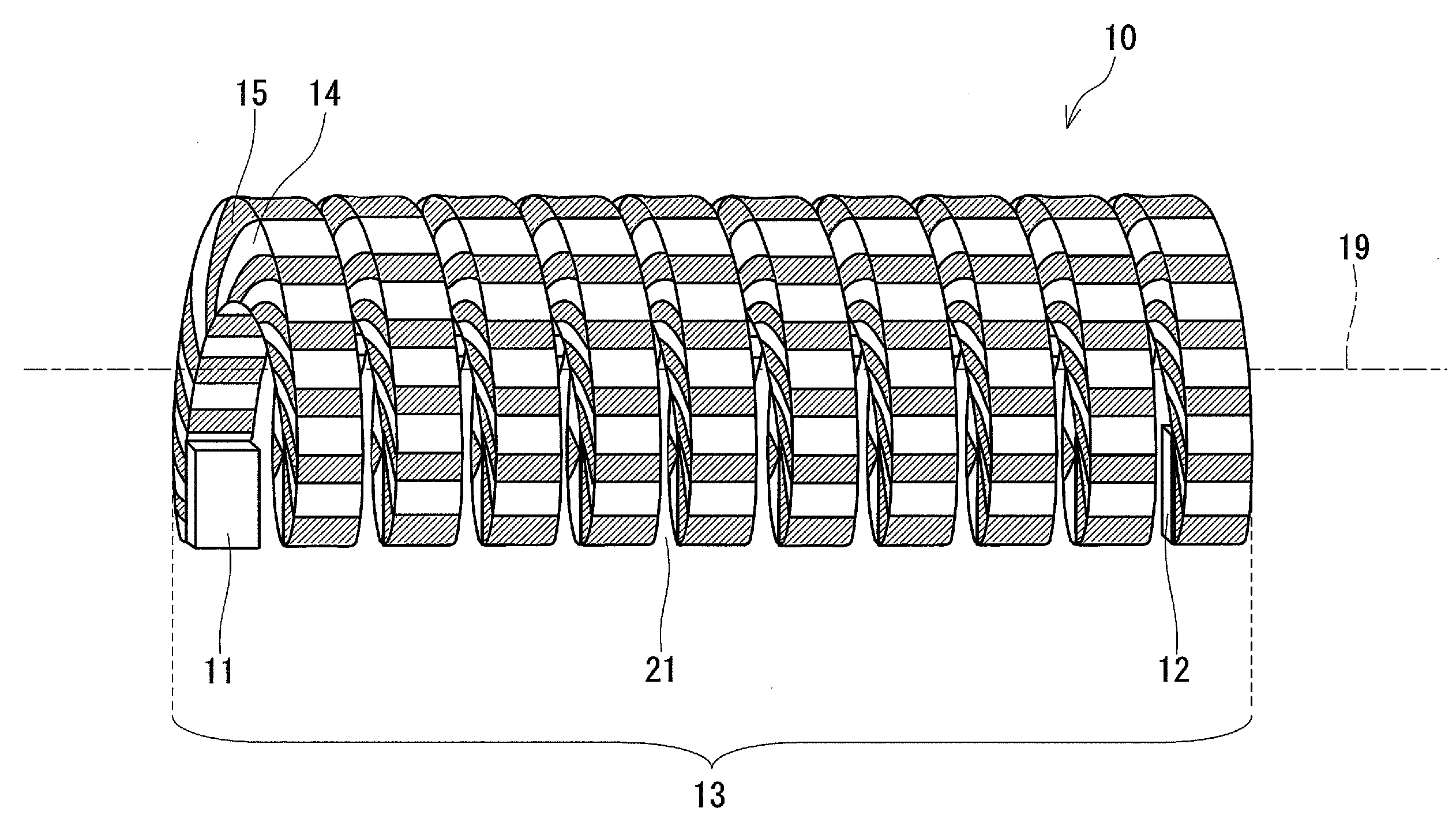
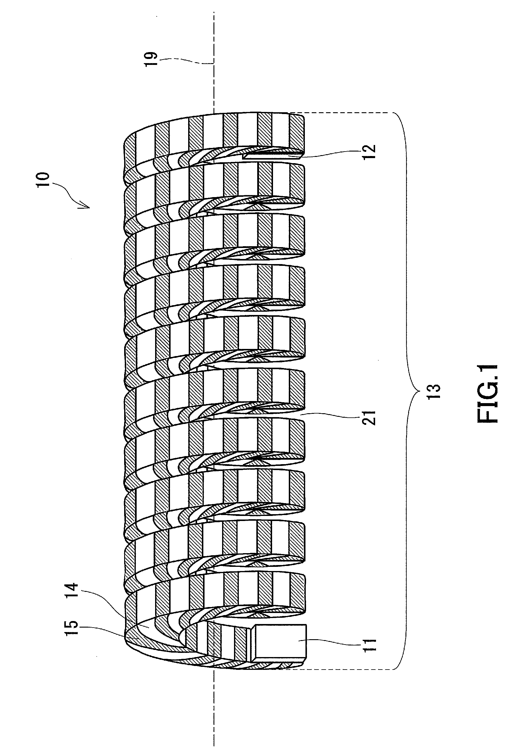
[0030]FIG. 1 is a diagram showing an example of a thermoelectric element according to the present invention. As shown in FIG. 1, the thermoelectric element 10 according to the present invention includes a laminate 13 as well as a first electrode 11 and a second electrode 12 that are disposed at both ends of the laminate 13, respectively. The laminate 13 has a shape surrounding a straight line axis 19 from one end to the other end and has a shape spirally extending around the axis 19. The laminate 13 is wound at sufficient intervals in the direction along the axis 19, with a space 21 being formed, so that the wound portions are not in contact with each other. The laminate 13 has a structure including first thermoelectric conversion material layers 14 and second thermoelectric conversion material layers 15 that are layered alternately from one end to the other end.
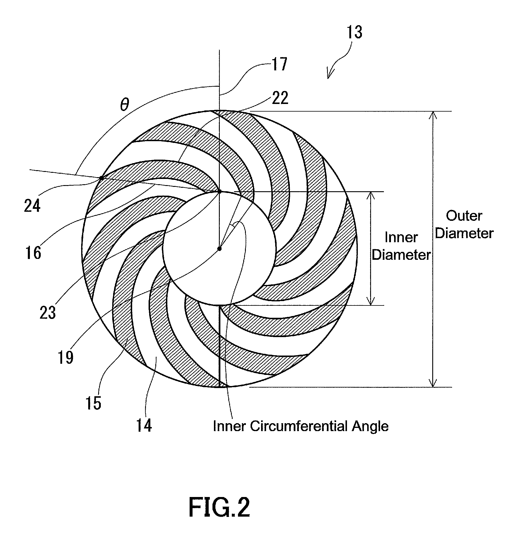
[0031]FIG. 2 is a diagram showing an example of a laminate of the thermoelectric element according to the present inventio...
embodiment 2
[0050]FIG. 7 is a diagram showing an example of a thermoelectric device according to the present invention. The thermoelectric device 70 has two laminates 13 that are connected electrically to each other. Since the structure of the laminate 13 was described in Embodiment 1, the description thereof is not repeated herein. One ends of the respective laminates 13 are connected electrically to each other through an interconnecting electrode 73. In each of the other ends of the respective laminates 13, an extracting electrode 71 is formed.
[0051]The materials for the extracting electrodes 71 and the interconnecting electrode 73 are not particularly limited, as long as materials with a high electrical conductivity are used. Specifically, a metal such as Cu, Ag, Mo, W, Al, Ti, Cr, Au, Pt, or In, a nitride such as TiN, or an oxide such as indium tin oxide (ITO) or SnO2 can be used. Furthermore, a solder, a silver brazing, or a conductive paste also may be used. The interconnecting electrode ...
example 1
[0058]A thermoelectric element 10 of Example 1 had the structure shown in FIG. 1, in which Cu was used as the material composing the first thermoelectric conversion material layers 14 and Bi was used as the material composing the second thermoelectric conversion material layers 15. The shape of the laminate 13 had an inner diameter of 100 mm, an outer diameter of 150 mm, and a width of 50 mm, and the ratio of the inner circumferential angles of Cu and Bi was 20:1. Furthermore, the angle θ was varied in the range of 0° to 240°. The width of the laminate 13 is the width in the direction along the axis 19.
[0059]The thermoelectric element 10 was produced by the production method shown in FIGS. 3D to 3F. First, a Cu plate with a size of 100 mm×100 mm and a thickness of 50 mm was subjected to cutting machining, and thereby thermoelectric conversion material layer pieces 31 with the same shape as that of the first thermoelectric conversion material layers 14 were produced (see FIGS. 3B and...
PUM
 Abstract
Description
Claims
Application Information