This helps you quickly interpret patents by identifying the three key elements:
Problems solved by technology
Method used
Benefits of technology
Benefits of technology
[0020]According to such a configuration, the blocking film is provided on the conducting paths, and therefore the fused eutectic alloy will not flow to the first and second exciting electrodes. Consequently, a reduction in crystal impedance, and the generation of spurious will not occur, and the resonating characteristics of the crystal resonator are thus maintained.
[0021]Moreover, the electrical connection between the crystal plate end surface electrode and the first base end surface electrode is made by joining the crystal plate auxiliary electrode and the base auxiliary electrode respectively connected thereto, using the eutectic alloy. Therefore, the crystal plate end surface electrode and the first base end surface electrode can easily be connected electrically. Moreover, there is no risk of failure in this eutectic alloy, and it is therefore possible to avoid electrical connectioncut between the crystal plate end surface electrode and the first base end surface electrode.
[0022]Furthermore, the width of the frame section of the framed crystal plate on one side on the one end side where the crystal plate auxiliary electrode is formed, differs from the width of the frame section at least on one other side. Therefore, a sufficient clearance can be made between the crystal plate auxiliary electrode and the second metallic film, and it is accordingly possible to prevent an electrical short by the eutectic alloy between the crystal plate auxiliary electrode and the second metallic film.
[0023]In the present invention, there is provided a configuration where the width of the frame section of the framed crystal plate on one side on the one end side where the crystal plate auxiliary electrode is formed, is greater than the width of the frame section of another side on the other end side.
[0024]Moreover, in the present invention, the one and other mount terminals are of a two-terminal configuration in which one of each terminal is arranged on both end sides and in the widthwise center of the base.
[0025]Furthermore, in the present invention, the one and other mount terminals are of a four-terminal configuration in which two of these terminals are respectively arranged on both sides of one same side.
Problems solved by technology
As a result, there will be negative effects on the resonating characteristics of the crystal resonator 1 such as a reduction in crystal impedance, and the generation of spurious.
However, the method of connecting the cutaway sections 9 (a, b) and the cutaway sections 14 (a, b) corresponding thereto using the eutectic alloy 19b is not reliable, and usually causes the manufacturing method of the crystal resonator 1 to become complex.
Method used
Image
Click on the blue label to locate the original text in one second.
Reading with bidirectional positioning of images and text.
Examples
first embodiment
Another Modified Example of First Embodiment
[0065]FIG. 5 includes drawings of a framed crystal plate in a stacked crystal resonator for describing another modified example of the first embodiment of the present invention, wherein FIG. 5A is a plan view of one principle surface of the crystal plate, and FIG. 5B is a plan view of the other principle surface thereof. The present modified example differs from the first embodiment in that the connecting sections 8 (a, b) are formed in opposing corners of the frame section 7 of the framed crystal plate 2. Other aspects thereof are the same as those of the first embodiment.
Second Embodiment
[0066]FIG. 6 and FIG. 7 are drawings for describing a second embodiment of a stacked crystal resonator of the present invention. FIG. 6A is a plan view of one principle surface of a framed crystal plate, FIG. 6B is a plan view of the other principle surface of the framed crystal plate, FIG. 7A is a plan view of one principle surface of a base, and FIG. 7...
second embodiment
Another Modified Example of Second Embodiment
[0076]FIG. 9 includes plan views of a framed crystal plate in a stacked crystal resonator for describing another modified example of the second embodiment of the present invention, wherein FIG. 9A is a plan view of one principle surface of the crystal plate, and FIG. 9B is a plan view of the other principle surface thereof. The same reference symbols are given to portions the same as those in the above embodiments, and descriptions thereof are simplified or omitted.
[0077]The present modified example differs from the second embodiment in the width of the frame section 7 of the framed crystal plate 2, and it is specifically described below. The film width of the second metallic film 13 is made, for example, 50 μm. The width of the frame section on one side having a cutaway section 9a and a cutaway section 9b on both ends thereof, and the width on the side opposite of this one side, are made, for example, 100 μm, which is close to the width ...
third embodiment
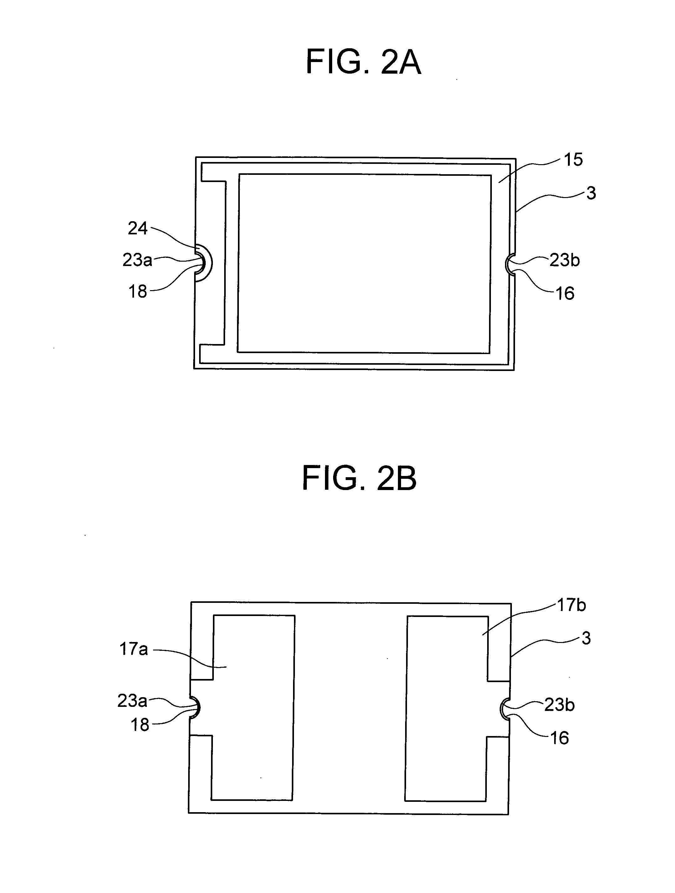
[0078]FIG. 10 and FIG. 11 are drawings of a stacked crystal resonator for describing a third embodiment of the present invention. FIG. 10A is a plan view of one principle surface of a framed crystal plate, FIG. 10B is a plan view of the other principle surface of the framed crystal plate, FIG. 11A is a plan view of one principle surface of a base, and FIG. 11B is a plan view of the other principle surface of the base. The same reference symbols are given to portions the same as those in the above embodiments, and descriptions thereof are simplified or omitted.
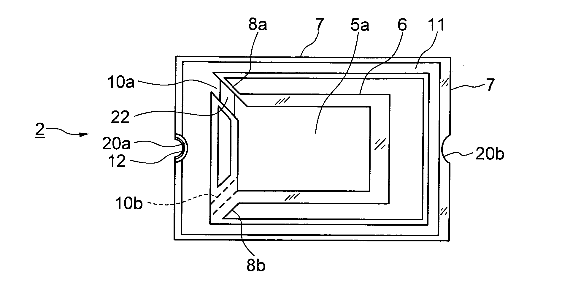
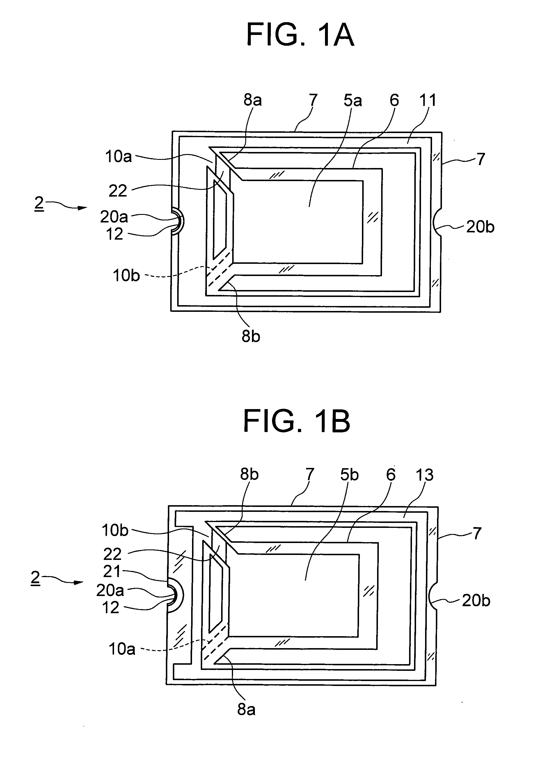
[0079]A stacked crystal resonator 1 is formed such that a ceramic-made base 3 and a metallic cover 4 are stacked on both of the principle surfaces of a framed crystal plate 2 (refer to FIG. 12). As shown in FIG. 10A and FIG. 10B, the framed crystal plate 2 includes a resonating section 6 having first and second exciting electrodes 5 (a, b) on both of the principle surfaces thereof, a frame section 7 that surrounds the resonatin...
PUM
Abstract
An object of the present invention is to provide a crystalresonator capable of maintaining its resonating characteristic and ensuring electrical connections between end surface electrodes using a simple method. Provided is a stacked crystalresonator including: a framed crystal plate, a frame section of which surrounds a resonating section, and to which both of these resonating section and frame section are connected by connecting sections; a first metallic film and second metallic film formed on both of the principle surfaces of the frame section of the framed crystal plate; and a base and cover stacked on both of the principle surfaces of the framed crystal plate. A crystal plate end surface electrode, which is electrically connected to the first metallic film, is electrically connected to a crystal plate auxiliary electrode; the crystal plate auxiliary electrode is electrically connected by a eutectic alloy while facing a base auxiliary electrode; the width of the frame section of one side on one end side of the framed crystal plate where the crystal plate auxiliary electrode is formed, differs from the width of the frame section of at least one other side; and a blocking film which blocks flow of the eutectic alloy to exciting electrodes, is provided on the conducting paths.
Description
BACKGROUND OF THE INVENTION[0001]1. Technical Field[0002]The present invention relates to a surface mount crystal resonator, in particular, to a stacked crystal resonator in which a crystal plate is stacked between a base and a cover.[0003]2. Background Art[0004]A surface mount crystal resonator is provided built-in particularly in portable electronic devices as a source of frequency reference or time reference because of its small size and light weight. Responding to the needs of the information-oriented society in recent years, consumption of surface mount resonators is high and consequently there is a demand for an improvement in the productivity thereof. An example of this type of crystal resonator is a stacked crystal resonator in which a framed crystal plate composed of a resonating section and a frame section that surrounds the resonating section is stacked between a base and a cover.PRIOR ART[0005]FIG. 12 to FIG. 14 are drawings for describing a conventional example of a sta...
Claims
Application Information
Patent Timeline
Application Date:The date an application was filed.
Publication Date:The date a patent or application was officially published.
First Publication Date:The earliest publication date of a patent with the same application number.
Issue Date:Publication date of the patent grant document.
PCT Entry Date:The Entry date of PCT National Phase.
Estimated Expiry Date:The statutory expiry date of a patent right according to the Patent Law, and it is the longest term of protection that the patent right can achieve without the termination of the patent right due to other reasons(Term extension factor has been taken into account ).
Invalid Date:Actual expiry date is based on effective date or publication date of legal transaction data of invalid patent.

