Modular camera system and a method of manufacturing the same

Active Publication Date: 2010-12-30
STMICROELECTRONICS RES & DEV +1
View PDF6 Cites 4 Cited by
  • Summary
  • Abstract
  • Description
  • Claims
  • Application Information

AI Technical Summary

Benefits of technology

[0006]This approach offers a number of benefits. It allows leverage of existing 3Mpix/5Mpix camera module designs. A high the level of functional integration is achieved. The design supports features of the processor as a stand-alone device. A single package solution is achieved which does not require a host system ISP. Imager/ISP integration is achieved in a single module. A complete approach is provided which can be tuned to optimize performance for the specific image/processor combination. The overall X/Y dimensions are smaller than that of a single die combining the imager and processor. A better isolation for noise and EMC purposes and an improved thermal performance is achieved

Problems solved by technology

Traditionally, an integrated camera system has not been possible due to incompatibility between the imager and processor die sizes, power dissipation, and substrate tracking density.

Method used


Image

  • Modular camera system and a method of manufacturing the same
  • Modular camera system and a method of manufacturing the same
  • Modular camera system and a method of manufacturing the same

Examples


Example

[0018]The present invention relates to a multichip modular camera based on stacking die and cavity substrates and making variations which permit a viable cavity bonding arrangement to support the functional combination of an imager and processor in a single package.

[0019]The following description and associated drawings describe the assembly of the module in stages focusing on the multichip ceramic cavity approach implemented within the design.

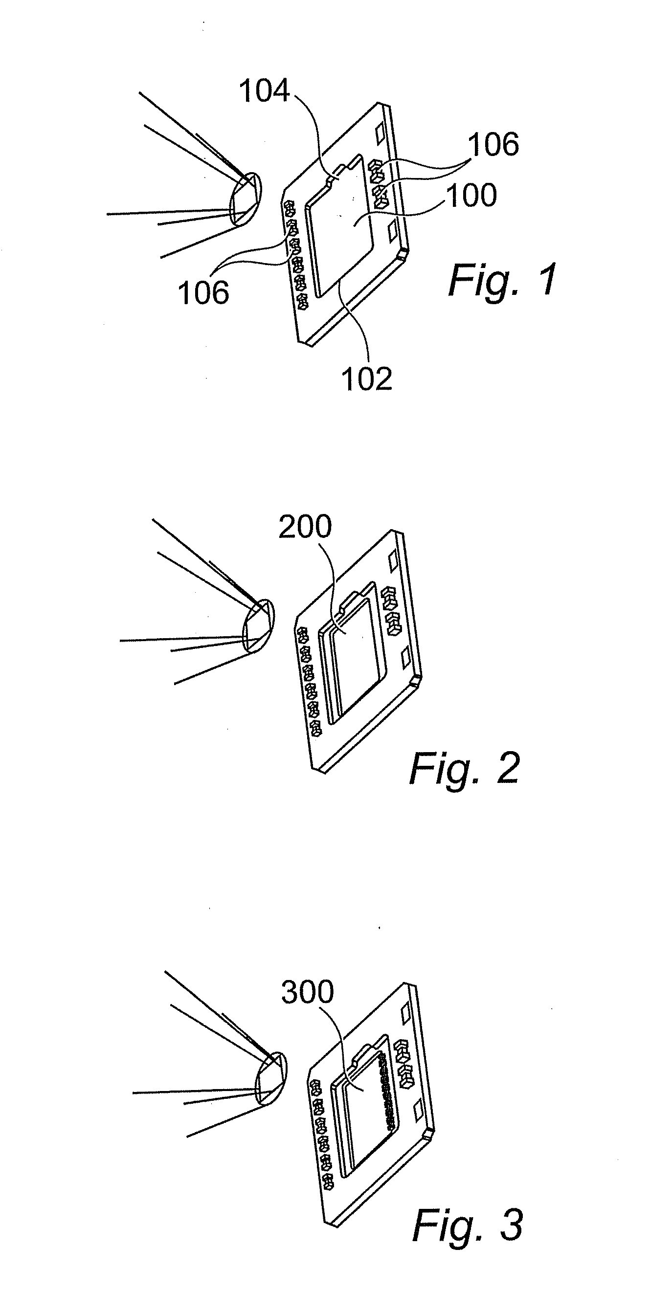
[0020]FIG. 1 shows a metalized ceramic module (MCM) ceramic substrate 100. The substrate includes a cavity 102 which is shaped to include a notch or cutout section 104. The notch is preferably relatively narrow to avoid unnecessary stresses being placed on the substrate during reliability tests. A typical width of the notch is in the region of 1.5 mm. The cavity along with the notch is punched out of the substrate by means of an appropriately shaped punch tool, after which the substrate is fired before the next steps are carried out. The cavit...


PUM

PropertyMeasurementUnit
Timeaaaaaaaaaa

Abstract

A camera module includes a substrate with a cavity therein. A processor is located in the cavity, and wire bonding is for connecting the processor to the substrate. An imaging module is adapted to overlay the processor in the cavity and rest on at least part of the edge of the cavity. Wire bonding is for connecting the imaging module to the substrate and the processor. The cavity includes a longitudinal cutout section adapted to accommodate at least some wire bonding for connecting the processor to the substrate or associated surface mount components.

Description

FIELD OF THE INVENTION[0001]The present invention relates to improvements in or relating to a modular camera system and a method of manufacturing the same.BACKGROUND OF THE INVENTION[0002]In the field of mobile communications the need for miniaturization and increased functionality and capability continues to grow. This has led to the desire to produce a functional camera system with an integrated image signal processor (ISP) in the camera module.[0003]Traditionally, an integrated camera system has not been possible due to incompatibility between the imager and processor die sizes, power dissipation, and substrate tracking density. In addition, combinations of image and processor have not been possible due to tracking and bonding requirements and constraints imposed by existing volume manufacturing capabilities.SUMMARY OF THE INVENTION[0004]It is an object of the present invention to produce a modular camera system with an integrated ISP.[0005]According to one aspect, there is a cam...

Claims


Application Information

Patent Timeline
IPC IPC(8): H04N5/225H05K3/30
CPCH01L27/14618Y10T29/4913H01L27/14683H01L2924/0002H01L2924/00
Inventor HALLIDAY, WILLIAMOOI, CHOON KIAT
Owner STMICROELECTRONICS RES & DEV
Why Eureka
Try Eureka