Memory controller for NAND memory using forward error correction

a memory controller and error correction technology, applied in the direction of fault response, static storage, instruments, etc., can solve the problems of introducing significant latency into the data read path, requiring significant circuit resources, and a large amount of computational resources, so as to achieve a high degree of error tolerance/detection, advantageously efficient, and low latency in the read path

Inactive Publication Date: 2010-12-30
ARM LTD
View PDF5 Cites 31 Cited by
  • Summary
  • Abstract
  • Description
  • Claims
  • Application Information

AI Technical Summary

Benefits of technology

[0012]The present technique provides error detecting circuitry with a form matched to the error characteristics of a NAND memory so as to provide an advantageously efficient overall system that yields a high degree of error tolerance / detection and yet introduces advantageously little latency in the read paths during normal use and consumes relatively little circuit resource. The rates A, B and C can each independently be variable or fixed, e.g. (i) the slow path having corrected Y errors can output the remaining error free data at rate B making the average rate C a data dependent (stochastic) variable; and / or (ii) the zero-error path and the i fast paths each have a different rate B which is greater than C making the rate B vary depending on the path(s) taken for a particular set of symbols.

Problems solved by technology

A problem with such memory is that symbol errors (e.g. bit errors) in the data read from the memory are relatively common, in particular for Multi-Level Cell (MLC) NAND memory, and tend to increase with time as the memory ages.
While such forward error correction is effective in coping with symbol errors, it is computationally intensive requiring significant circuit resource and introducing significant latency into the data read paths.

Method used


Image

  • Memory controller for NAND memory using forward error correction
  • Memory controller for NAND memory using forward error correction
  • Memory controller for NAND memory using forward error correction

Examples


Embodiment Construction

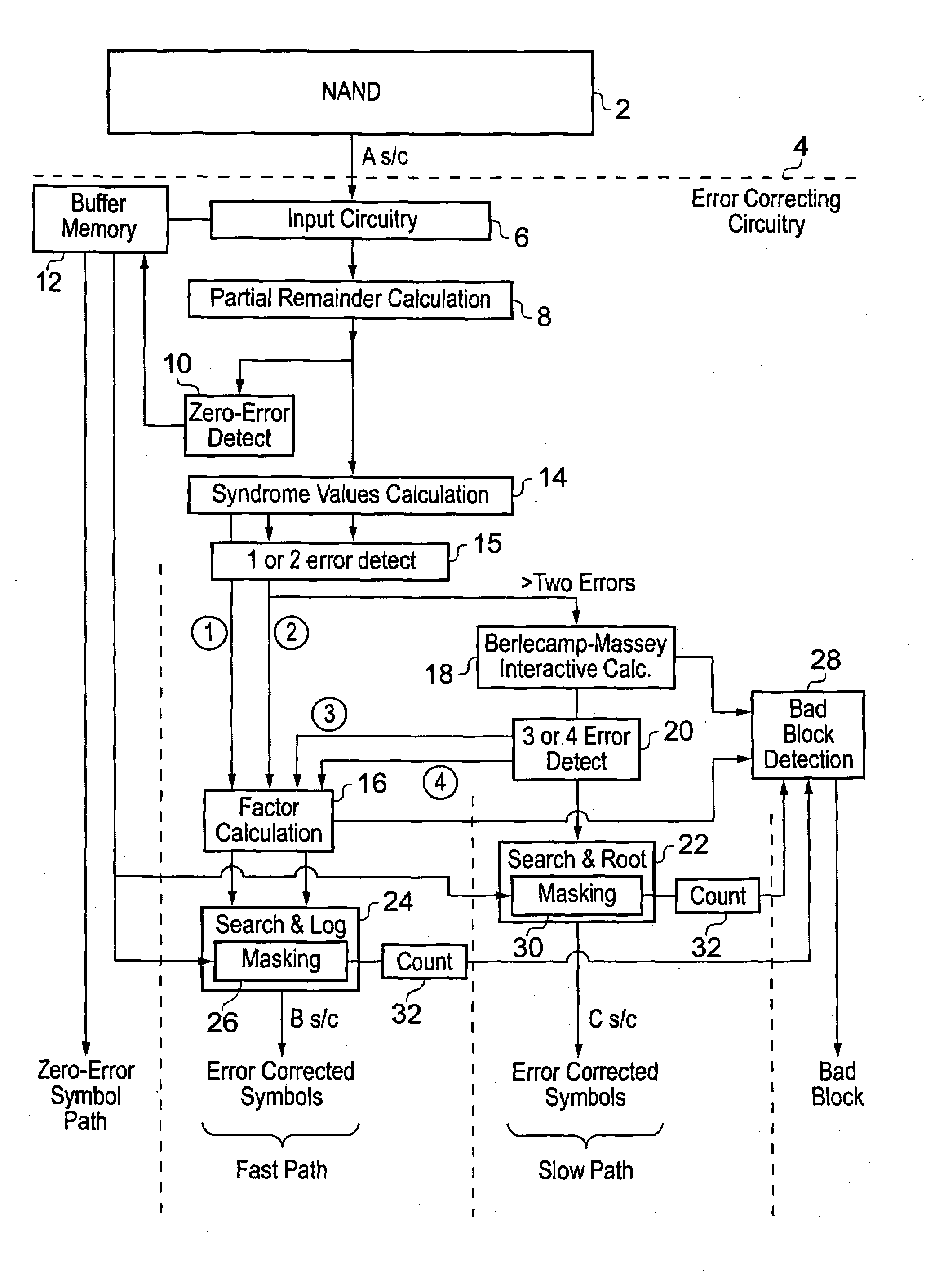
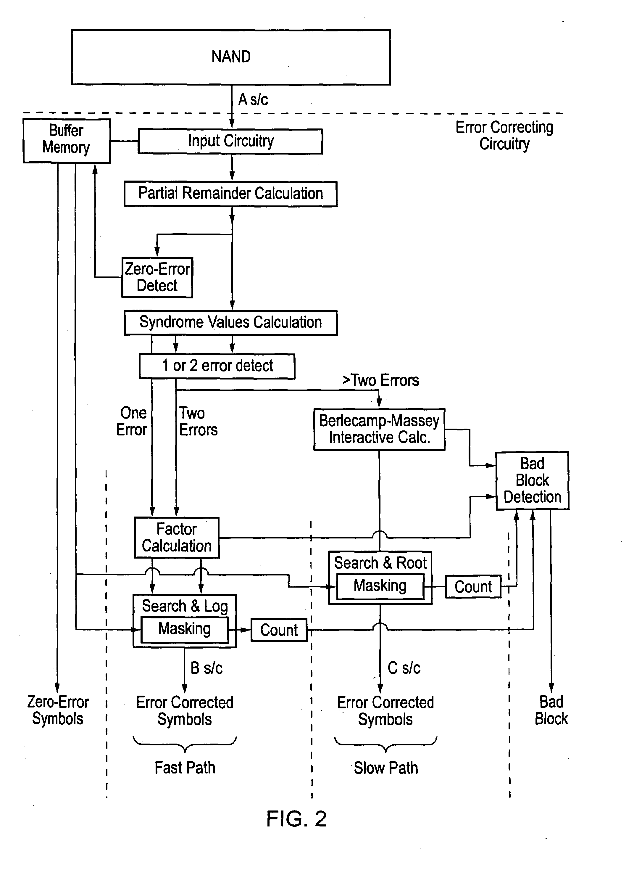
[0026]FIG. 1 schematically illustrates a first embodiment of a system including a NAND memory array 2 coupled to a memory controller 4 that includes error detecting circuitry. The error detecting circuitry includes input circuitry 6 for accepting blocks of symbols as a stream of symbols at a rate of A symbols per cycle and forwarding the data to both partial remainder calculating circuitry 8 and a buffer memory 12. The parity symbols are only forwarded to the partial remainder calculating circuitry 8. The partial remainder calculating circuitry 8 receives the symbols read from the NAND memory and calculates Q partial remainder values resulting from dividing the block of symbols by one of Q factors of a generator polynomial (which defines the used BCH code) and Q products of factors of a generator polynomial, Q being an integer greater than 1 and the partial remainder values being indicative of any symbol-errors within the block of symbols.

[0027]Fast zero-detecting circuitry 10 is co...


PUM


Abstract

A memory controller 4 for a NAND memory array 2 includes error detecting circuitry having input circuitry 6, fast zero-error detecting circuitry 10, fast-path error correcting circuitry 16, 24, slow-path error correcting circuitry 18, 22 and fast-bad-block detecting circuitry 28.

Description

BACKGROUND OF THE INVENTION[0001]1. Field of the Invention[0002]This invention relates to the field of memory controllers for reading NAND memory. More particularly, this invention relates to memory controllers for reading NAND memory that employ forward error correction.[0003]2. Description of the Prior Art[0004]It is known to utilise NAND memory to provide high density, low cost storage in many recent data processing systems. A problem with such memory is that symbol errors (e.g. bit errors) in the data read from the memory are relatively common, in particular for Multi-Level Cell (MLC) NAND memory, and tend to increase with time as the memory ages.[0005]In order to deal with this type of symbol error it is known to provide techniques such as forward error correction (FEC) that add redundant data to data stored so as to enable symbol errors to be detected and corrected. While such forward error correction is effective in coping with symbol errors, it is computationally intensive r...

Claims


Application Information

Patent Timeline
Patent Type & Authority Applications(United States)
IPC IPC(8): G11C29/04G06F11/07
CPCG06F11/1048G11C2029/0411G11C2029/0409
Inventor WEZELENBURG, MARTINUS CORNELISCONWAY, THOMAS KELSHAWSYMES, DOMINIC HUGO
Owner ARM LTD
Why Eureka
Try Eureka