Method and computer system for optimizing the signal time behavior of an electronic circuit design

a technology of electronic circuits and signal time behavior, applied in the field of electronic circuit design and manufacture, can solve the problems of not being able to create clones of sequential logic circuits, the checker tools that can compare sequential logic circuits are not ready for use in today's design process, and the clock tree construction has become a challenging problem, so as to achieve the effect of high latency

Inactive Publication Date: 2010-11-30
TAIWAN SEMICON MFG CO LTD
View PDF9 Cites 6 Cited by
  • Summary
  • Abstract
  • Description
  • Claims
  • Application Information

AI Technical Summary

Benefits of technology

[0027]It is an advantage of the method and the program according to the present invention that no manual interaction is needed and a high degree of circuit design automation is achieved. Alternative sub-clock tree information is kept for the main clock tree construction and allows reacting to the inflexibility and the constraints of fixed circuits when generating implementations of a main clock tree. As a result the handling of multiple alternative implementations allows generating a configuration with a minimum latency.
[0035]Alternative implementations may differ for example in the following way: one implementation provides a low power level and a small latency and another implementation provides a higher power level but a higher latency.

Problems solved by technology

Due to the increase of clock frequencies and design sizes clock tree construction has become a challenging problem in the design of ICs.
Then the problem exists, that the modified ASIC design comprising the additional test logic needs to be functionally equivalent to the ASIC design without the test logic.
Checker tools that are able to compare sequential logic circuits are still not ready for usage in today's design processes.
Therefore, it is not desired that clones of these circuits are created because this would have a negative impact on the timing of the gating signal.
The general problem of constructing a configuration of at least one logic structure, preferably of clock tree construction, is the task of parallel and serial repowering of one or multiple logic structures such that the given target arrival time windows at all sinks are achieved.
Clock tree construction, especially in the presence of fixed circuits in between clock trees or clock tree parts usually is a difficult and manual task.

Method used


Image

  • Method and computer system for optimizing the signal time behavior of an electronic circuit design
  • Method and computer system for optimizing the signal time behavior of an electronic circuit design
  • Method and computer system for optimizing the signal time behavior of an electronic circuit design

Examples


Embodiment Construction

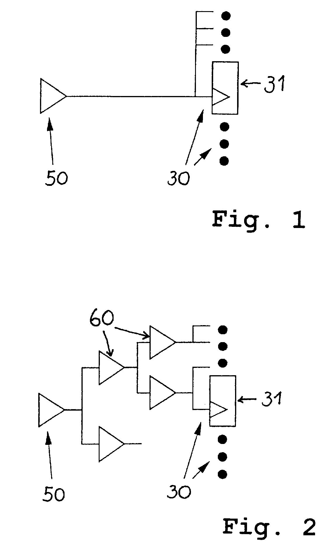
[0046]FIG. 1 shows a configuration before building a clock tree. The configuration comprises a root driver 50 and several sinks 30, symbolized by black dots, as well as a sink 31, which may be for example, a latch or a RAM.

[0047]FIG. 2 shows a configuration after building a clock tree. A clock tree can have multiple roots though this is not illustrated in the figures. The parallel and serial repowering is typically performed by inserting buffers and / or inverters 60.

[0048]Generally, any circuit which is necessary in a clock tree and which has multiple inputs, e.g. a clock gating circuit, may be cloned. Algorithms for building zero-skew clock trees and skew-scheduled clock trees are known from Held S., Korte B., Maβberg J., Ringe M., Vygen J.: “Clock Scheduling and Clock Tree Construction for High Performance ASICs”, Proceedings of the International Conference on Computer Aided Design, 232-239, 2003.

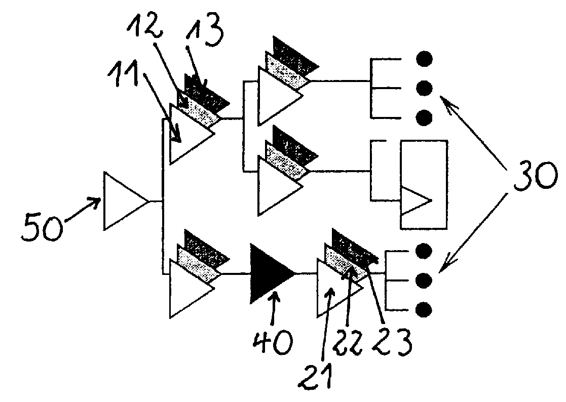
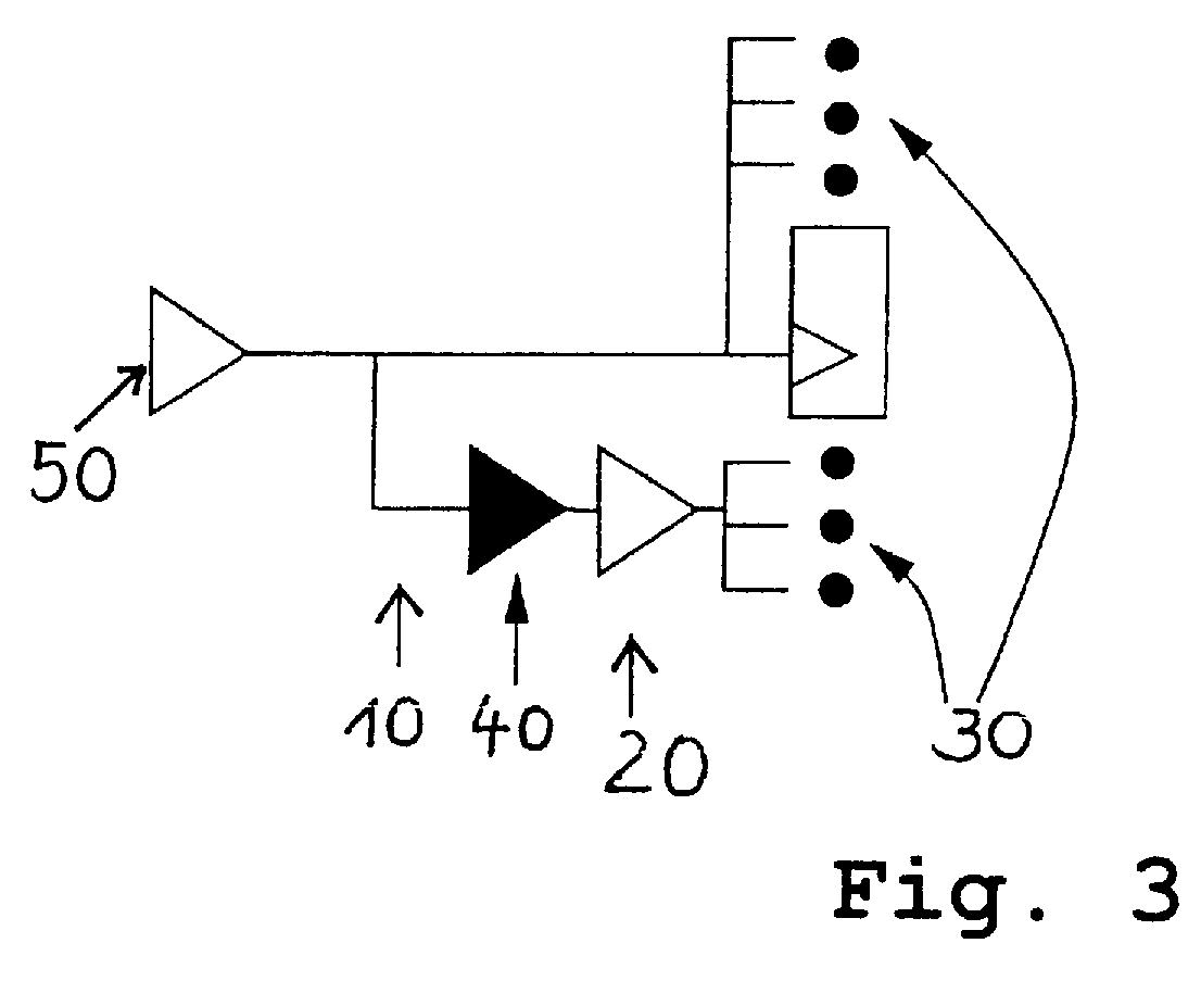
[0049]FIG. 3 shows a configuration which additionally incorporates a fixed circuit 40 ...


PUM


Abstract

A method and program for designing an electronic circuit, especially a clock tree and a sub-clock tree, within a set of sinks with given target arrival time windows, preferably on an integrated circuit. The clock tree and the sub-clock tree are preferably connected through one or multiple fixed circuits which must not be altered, cloned or removed. Several alternative implementations of the at least one logic structure are built and for each of the several alternative implementations data is stored. A set of configurations is built, each configuration comprising a combination of the one or several alternative implementations and each configuration satisfying the target arrival time windows at the complete set of sinks. A configuration is selected according to an evaluation of the data, preferably latency data, for constructing the configuration. No manual interaction is needed and a configuration with minimum latencies is provided.

Description

CROSS-REFERENCES TO RELATED APPLICATIONS[0001]This application is related to European Patent application Number 07103339.3, filed Mar. 1, 2007, and U.S. patent application Ser. No. 12 / 032,734, filed Feb. 18, 2008. All related Applications referenced above have common inventors and are assigned to the same assignee.BACKGROUND OF THE INVENTION[0002]The present invention relates to the field of electronic circuit design and manufacture, especially to semiconductor circuits.[0003]An integrated circuit (“IC”) is a semiconductor device that includes many electronic components (e.g., transistors, diodes, inverters, etc.). These electrical components are interconnected to form larger scale circuit components (e.g., gates, cells, memory units, arithmetic units, controllers, decoders, etc.) on the IC.[0004]Design engineers create an IC by transforming a circuit description of the IC into a geometric description called a “layout”. To create an IC layout, design engineers typically use electron...

Claims


Application Information

Patent Timeline
Patent Type & Authority Patents(United States)
IPC IPC(8): G06F17/50
CPCG06F17/5068G06F2217/62G06F2217/84G06F30/396G06F2119/12G06F30/39
Inventor HUTZL, GUENTHERHELD, STEPHANKOEHL, JUERGENKORTE, BERNHARDMASSBERG, JENSRINGE, MATTHIASVYGEN, JENS
Owner TAIWAN SEMICON MFG CO LTD
Why Eureka
Try Eureka