Light-Emitting Device, Lighting Device, and Electronic Device
Active Publication Date: 2011-01-06
SEMICON ENERGY LAB CO LTD
View PDF47 Cites 240 Cited by
Summary
Abstract
Description
Claims
Application Information
AI Technical Summary
This helps you quickly interpret patents by identifying the three key elements:
Problems solved by technology
Method used
Benefits of technology
Benefits of technology
[0013]In view of the foregoing problem, it is an object of an embodiment of the present invention to provide a flexible light-emitting device with high reliability in a simple way. Further, it is an object to provide an electronic device or a lighting device each mounted with the light-emitting device.
[0024]In accordance with an embodiment of the present invention, a light-emitting device which has high reliability and is thinned can be provided. Further, in accordance with an embodiment of the present invention, a lighting device or an electronic device with high reliability can be provided with the use of a light-emitting device with high reliability.
Problems solved by technology
However, in commercialization of such a flexible light-emitting device, the biggest problem is its lifetime.
The reason of the problem is that, in a flexible light-emitting device, a plastic substrate has to be used as a support substrate which needs to support a light-emitting element and to protect an element against moisture, oxygen, and the like in the outside thereof.
In Non-Patent Document 1, for example, an example in which a light-emitting element is formed over a substrate including polyethersulfone (PES) as a base and is sealed with an aluminum film to form a flexible light-emitting device is introduced; however, its lifetime is about 230 hours and the light-emitting device is miles away from commercialization.
In this example, moisture and the like are prevented from entering from the stainless steel substrate side; however, moisture cannot be prevented effectively from entering from the light-emitting element side.
Method used
Image
Click on the blue label to locate the original text in one second.
Reading with bidirectional positioning of images and text.
Examples
embodiment 1
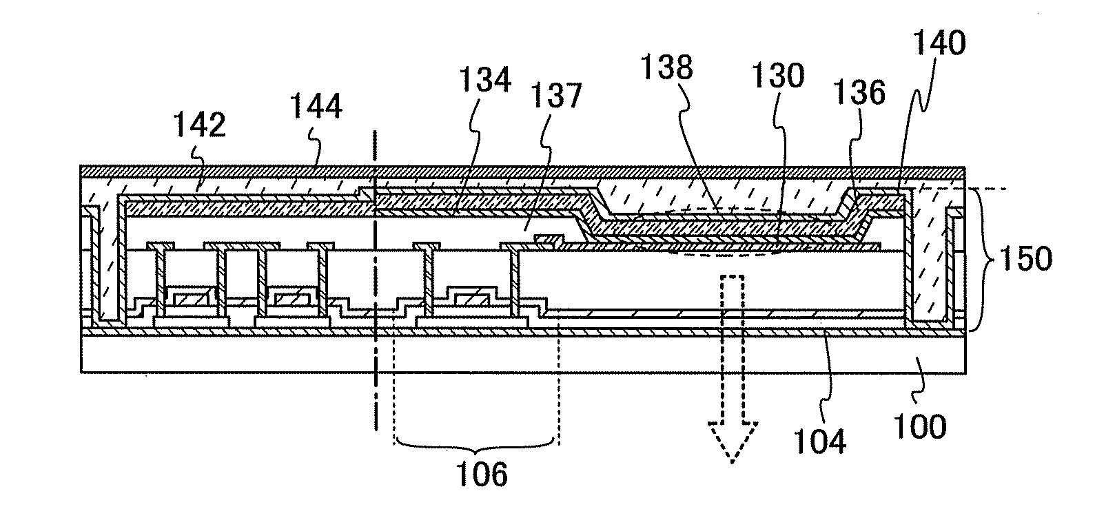
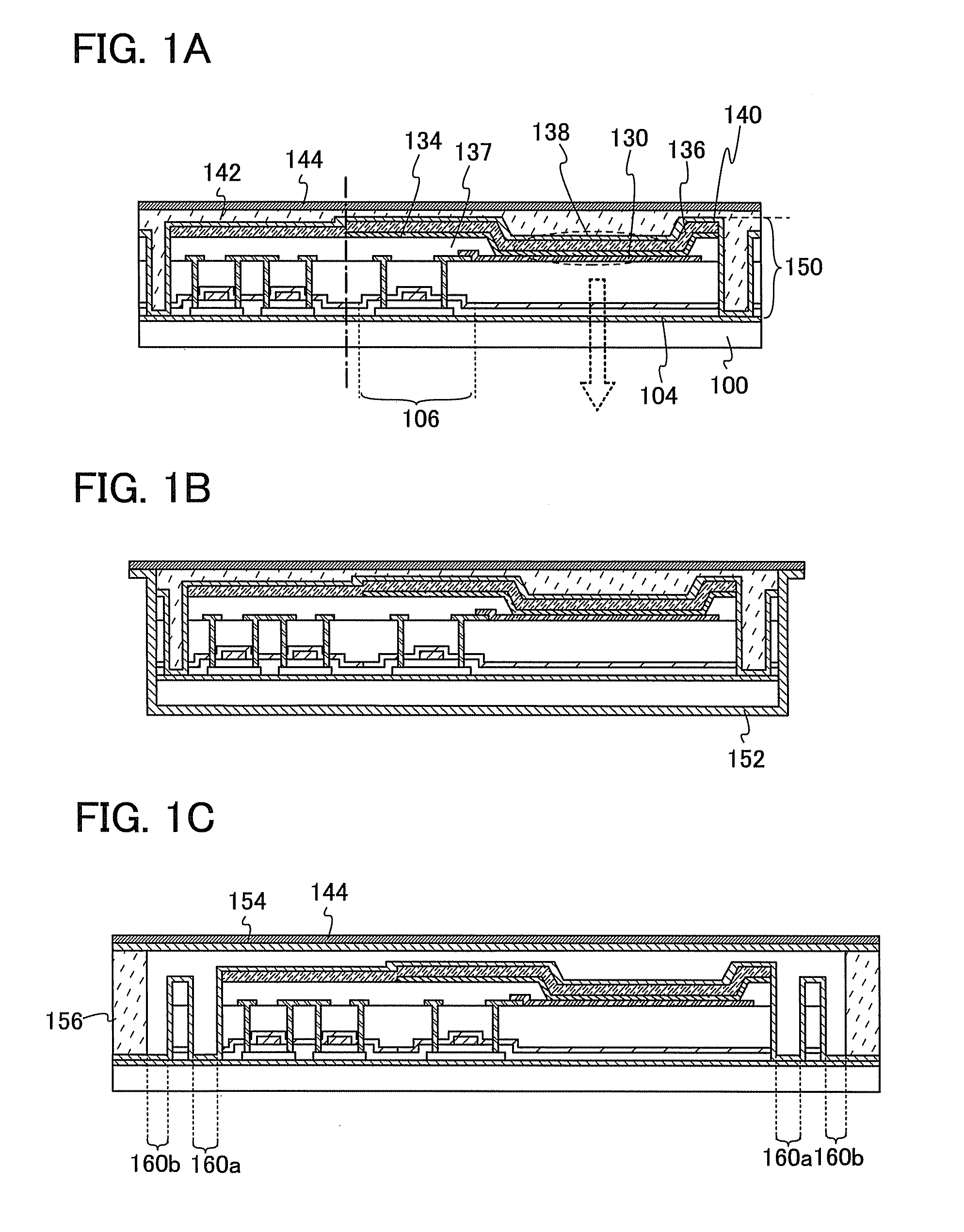
[0035]In this embodiment, examples of a light-emitting device will be described with reference to FIGS. 1A to 1C. FIGS. 1A to 1C each illustrate a display portion of a light-emitting device of this embodiment.
[0036]The light-emitting device of this embodiment which is illustrated in FIG. 1A includes an element portion 150 and a first insulating layer 104 over a substrate 100. A top surface and a side surface of the element portion 150 are covered with a second insulating layer 140. Further, at least parts of the first insulating layer 104 and the second insulating layer 140 are in contact with each other in end portions of the light-emitting device where the element portion 150 is not present, so that the element portion 150 is sealed. Note that it is preferable that the first insulating layer 104 and the second insulating layer 140 be in contact with each other so as to surround the outer periphery of the element portion 150, and it is still preferable that a region where the first...
embodiment 2
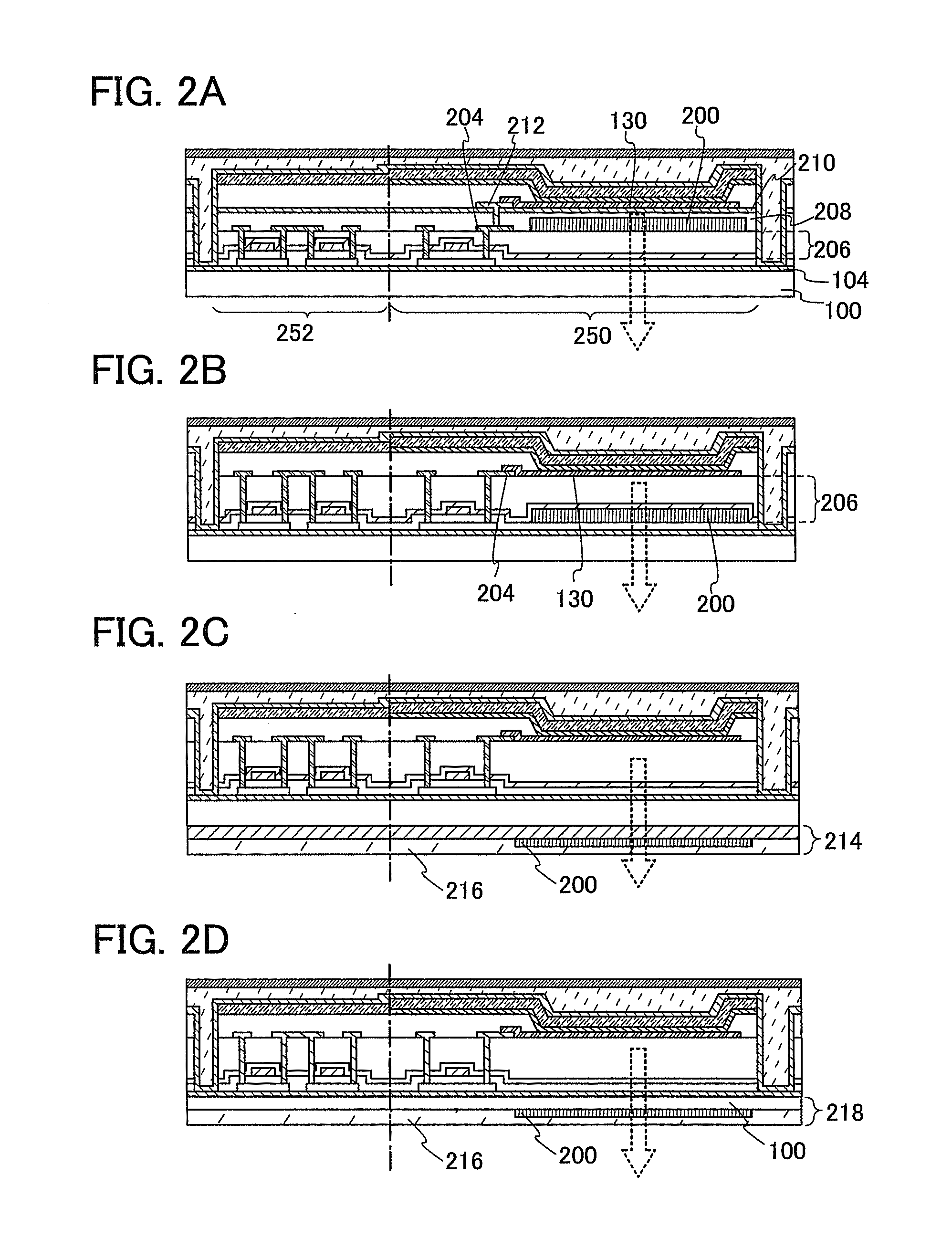
[0070]An example of a method for manufacturing a light-emitting device an embodiment of which is shown in Embodiment 1 is described with reference to FIGS. 3A to 3C, FIGS. 4A to 4D, and FIGS. 5A and 5B. In this embodiment, the case of manufacturing the structure of the light-emitting device illustrated in FIG. 1A is described as an example.
[0071]First, a separation layer 302 is formed over a substrate 300 having an insulating surface, which is a formation substrate, and subsequently, the first insulating layer 104 is formed. The separation layer 302 and the first insulating layer 104 can be formed in succession. By forming successively, the surface of the separation layer 302 is not exposed to the air, so that impurities can be prevented from being contained in the separation layer 302 and the first insulating layer 104.
[0072]As the substrate 300, which is a formation substrate, a glass substrate, a quartz substrate, a sapphire substrate, a ceramic substrate, a metal substrate havin...
embodiment 3
[0122]In this embodiment, a structure of a light-emitting element included in a light-emitting device is specifically described with reference to FIGS. 6A to 6C.
[0123]FIG. 6A illustrates an example of the structure of a light-emitting element. In the light-emitting element of FIG. 6A, the EL layer 134 is provided between the first electrode 130 and the second electrode 136. Note that there is no particular limitation on a stacked-layer structure of the EL layer 134 as long as a light-emitting layer is included. The EL layer 134 may be formed in an appropriate combination of a light-emitting layer with a layer containing a substance having a high electron transport property, a layer containing a substance having a high hole transport property, a layer containing a substance having a high electron injection property, a layer containing a substance having a high hole injection property, a layer containing a bipolar substance (a substance having high electron transport and hole transpor...
PUM
Abstract
It is an object to provide a flexible light-emitting device with high reliability in a simple way. Further, it is an object to provide an electronic device or a lighting device each mounted with the light-emitting device. A light-emitting device with high reliability can be obtained with the use of a light-emitting device having the following structure: an element portion including a light-emitting element is interposed between a substrate having flexibility and a light-transmitting property with respect to visible light and a metal substrate; and insulating layers provided over and under the element portion are in contact with each other in the outer periphery of the element portion to seal the element portion. Further, by mounting an electronic device or a lighting device with a light-emitting device having such a structure, an electronic device or a lighting device with high reliability can be obtained.
Description
BACKGROUND OF THE INVENTION[0001]1. Field of the Invention[0002]The present invention relates to a light-emitting device including a light-emitting element utilizing electroluminescence (EL). Further, the present invention relates to a lighting device manufactured using the light-emitting device, or to an electronic device in which a display portion is mounted with the light-emitting device.[0003]2. Description of the Related Art[0004]In recent years, a light-emitting device to be mounted in a display of a television set, a mobile phone, a digital camera, or the like, or in a lighting device has been required to be flat and thin. A light-emitting device utilizing a self-luminous light-emitting element has attracted attention as a light-emitting device for meeting this requirement. One of the self-light-emitting elements is a light-emitting element utilizing electroluminescence, and this light-emitting element includes a light-emitting material interposed between a pair of electrodes...
Claims
Application Information
Patent Timeline
Application Date:The date an application was filed.
Publication Date:The date a patent or application was officially published.
First Publication Date:The earliest publication date of a patent with the same application number.
Issue Date:Publication date of the patent grant document.
PCT Entry Date:The Entry date of PCT National Phase.
Estimated Expiry Date:The statutory expiry date of a patent right according to the Patent Law, and it is the longest term of protection that the patent right can achieve without the termination of the patent right due to other reasons(Term extension factor has been taken into account ).
Invalid Date:Actual expiry date is based on effective date or publication date of legal transaction data of invalid patent.

