Electronic component

a technology of electronic components and components, applied in the field of electronic components, can solve the problems of short circuit failure between the outer electrodes and the likely event of short circuit failure due to the migration of ag, and achieve the effect of preventing short circuit failur

Active Publication Date: 2011-01-06
MURATA MFG CO LTD
View PDF5 Cites 9 Cited by
  • Summary
  • Abstract
  • Description
  • Claims
  • Application Information

AI Technical Summary

Benefits of technology

[0009]To overcome the problems described above, preferred embodiments of the present invention provide an electronic component which is capable of being mounted by using conductive adhesive and in which short circuit failure is prevented.

Problems solved by technology

However, short circuit failure between the outer electrodes can be caused due to migration of Ag in the multilayer ceramic electronic component disclosed in Japanese Unexamined Patent Application Publication No. 2002-158137.
In particular, when the multilayer ceramic electronic component disclosed in Japanese Unexamined Patent Application Publication No. 2002-158137 is used in a high temperature atmosphere of, for example, about 150° C. or greater, as in a case in which the multilayer ceramic electronic component is used in or near an engine control unit (ECU) in an automobile, the short circuit failure due to the migration of Ag is likely to occur.

Method used


Image

  • Electronic component
  • Electronic component
  • Electronic component

Examples


first preferred embodiment

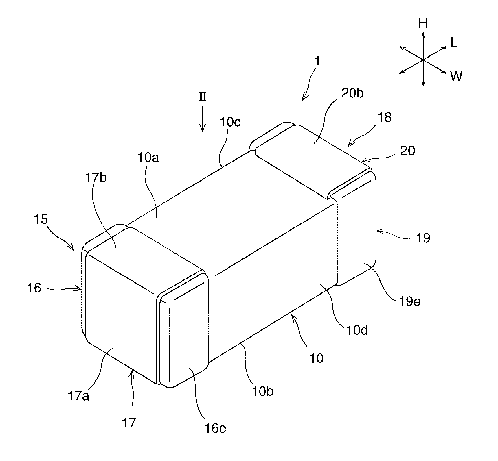
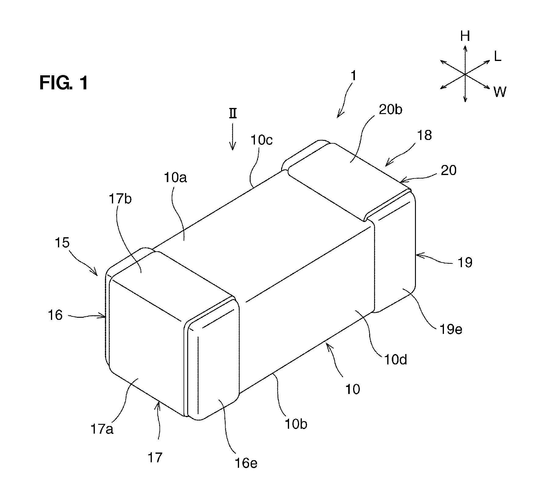
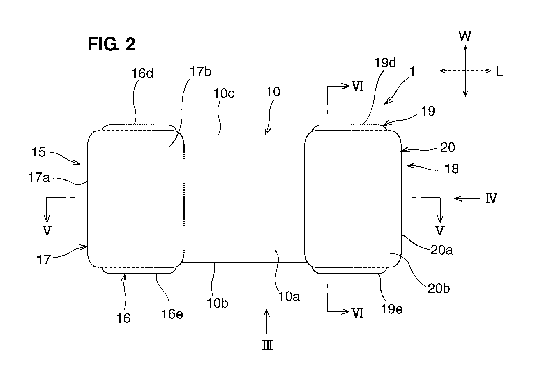
[0044]FIG. 1 is a schematic perspective view of an electronic component according to a first preferred embodiment of the present invention. FIG. 2 is a schematic plan view of the electronic component according to the first preferred embodiment of the present invention. FIG. 3 is a schematic side view of the electronic component according to the first preferred embodiment of the present invention, viewed from an arrow III in FIG. 2. FIG. 4 is a schematic front view of the electronic component, according to the first preferred embodiment of the present invention viewed from an arrow IV in FIG. 2. FIG. 5 is a schematic cross-sectional view of the electronic component, taken along a line V-V in FIG. 2. FIG. 6 is a schematic cross-sectional view of the electronic component, taken along a line VI-VI in FIG. 3. FIG. 7 is a schematic cross-sectional view of the electronic component, taken along a line VII-VII in FIG. 5. FIG. 8 is a schematic cross-sectional view of the electronic component,...

second preferred embodiment

[0100]The first to fourth inner conductors 13a, 14a, 13b, and 14b are preferably connected to the first outer electrode 15 or the second outer electrode 18 in the above first preferred embodiment. However, the present invention is not limited to this structure. According to a second preferred embodiment of the present invention, the first to fourth inner conductors 13a, 14a, 13b, and 14b may preferably be connected to none of the first outer electrode 15 and the second outer electrode 18, as shown in FIG. 14. With this configuration, an occurrence of the migration of Ag can be prevented, as in the first preferred embodiment. Accordingly, it is possible to prevent an occurrence of short circuit failure.

third preferred embodiment

[0101]One first inner conductor 13a, one second inner conductor 14a, one third inner conductor 13b, and one fourth inner conductor 14b are preferably provided in the above first preferred embodiment. However, the present invention is not limited to this structure. According to a third preferred embodiment of the present invention, multiple first inner conductors 13a, multiple second inner conductors 14a, multiple third inner conductors 13b, and multiple fourth inner conductors 14b may preferably be provided along the vertical direction. For example, as shown in FIG. 15, two first inner conductors 13a, two second inner conductors 14a, two third inner conductors 13b, and two fourth inner conductor 14b may be arranged along the vertical direction. The provision of the multiple first inner conductors 13a, the multiple second inner conductors 14a, the multiple third inner conductors 13b, and the multiple fourth inner conductors 14b along the vertical direction H allows an occurrence of t...


PUM


Abstract

An electronic component includes an electronic component body, first and second outer electrodes, and first and second inner electrodes. The first outer electrode includes a first conductive layer that does not include silver and a second conductive layer that is deposited on the first conductive layer so as to be positioned at an outermost layer and that includes silver. The second conductive layer includes a first contact portion in contact with a first main surface and is not in contact with first and second side surfaces. A first inner conductor is provided on a virtual straight or substantially straight line connecting a second inner electrode closest to the first contact portion and the first contact portion in the shortest distance. The first inner conductor is connected only to the first outer electrode or is connected to none of the first and second outer electrodes.

Description

BACKGROUND OF THE INVENTION[0001]1. Field of the Invention[0002]The present invention relates to electronic components and, more particularly, to an electronic component including inner electrodes and outer electrodes including silver (Ag).[0003]2. Description of the Related Art[0004]Many electronic components, such as ceramic electronic components, are mounted on a wiring board installed in an electronic device. Although solder including lead (Pb) is generally used in the mounting of such electronic components on a wiring board in related art, an attempt to mount electronic components without using Pb is presently being pursued in order to reduce environmental loads.[0005]For example, methods of mounting electronic components using conductive adhesive in which conductive fine particles, such as metallic filler, are added to thermosetting resin, such as thermosetting epoxy resin, or Pb-free solder are commonly used in order to mount the electronic components without using Pb. Variou...

Claims


Application Information

Patent Timeline
Patent Type & Authority Applications(United States)
IPC IPC(8): H01L41/00H01G4/005H01C7/13H01G4/232H01G4/30
CPCH01C1/14H01L41/047H01G4/005H01C7/008H10N30/871H10N30/872H10N30/877
Inventor OGUNI, TOSHIMIARITOMI, KATSUTOMO
Owner MURATA MFG CO LTD
Why Eureka
Try Eureka