Pad structure of integrated circuit package

A technology of integrated circuits and pads, which is applied in the field of connection pad structures and pad structures, and can solve problems such as short circuit faults, solder inability to overflow, and difficulty in meeting assembly and welding process requirements.

Active Publication Date: 2012-11-07
FUJIAN MINHANG ELECTRONICS
View PDF5 Cites 8 Cited by
  • Summary
  • Abstract
  • Description
  • Claims
  • Application Information

AI Technical Summary

Problems solved by technology

However, with the continuous advancement of the thinning and miniaturization of electronic components, the pitch of the external leads (ie pads) of the ceramic chip carrier package has changed from 1.27mm, 1.00mm to 0.80mm, 0.60mm, 0.50mm, 0.40mm Even smaller pitches are advanced. When the pad pitch is less than 1.00mm, the size of the semicircular metallized through hole of the ceramic shell has to be made extremely small. At this time, it is difficult to meet the requirements of the assembly and welding process: the solder cannot overflow during assembly, and the remaining Metal solder particles and flux are difficult to clean off, resulting in a decrease in insulation performance and even a short circuit fault. Residual solder and flux also lead to a sharp drop in soldering strength
This means that the ceramic package with a pitch of 1.00mm and above is equipped with a semi-circular metallized through-hole overflow structure, which is difficult to meet the assembly and welding requirements of ceramic packages with a pitch of 0.80mm and below

Method used


Image

  • Pad structure of integrated circuit package

Examples


Embodiment Construction

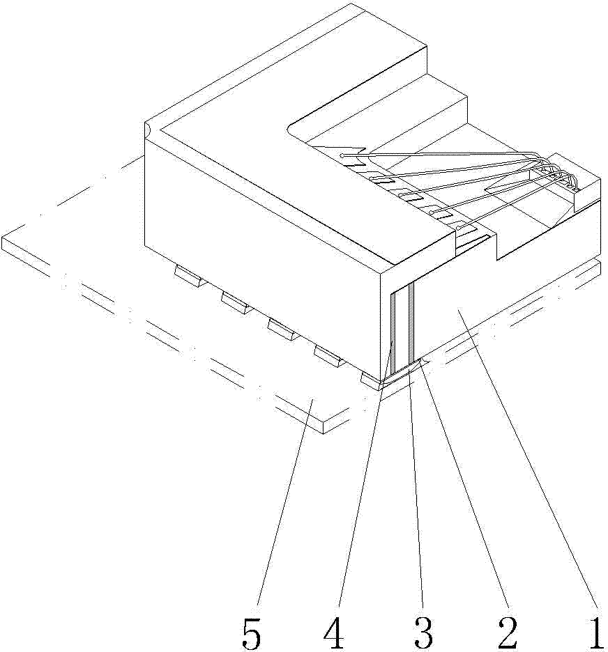
[0011] figure 1 A specific embodiment of the pad structure of an integrated circuit package of the present invention is given, which includes a ceramic shell 1, a pad 2, a bump 3 and an interconnection blind hole 4, and the internal wiring of the ceramic shell 1 passes through the interconnection blind hole 4 is connected to the pad 2 to meet the requirements for fine-pitch interconnection; the bump 3 is located on the pad 2 and protrudes from the surface of the ceramic shell 1, and various solder bumps 3 can be made on the surface of the pad 2, or can be made on the surface of the pad 2 Various metal protrusions 3 are sintered or welded on the pad 2. The height of the protrusions 3 protruding from the surface of the ceramic shell 1 is not limited. The height of the protrusions is preferably 0.1-0.5 mm, preferably 0.15 mm-0.25 mm. The surface of the ceramic case 1 is generally flush with the surface of the pad 2, so the height of the protrusion 3 protruding from the surface of...


PUM


Abstract

The invention discloses a pad structure of integrated circuit package, in particular to a connection pad structure between a fine-pitch lead-free plate-type carrier ceramic package lead-out end and a circuit board. The pad structure comprises a ceramic casing 1, a pad 2, a protrusion 3 and an interconnection blind hole 4, internal wiring of the ceramic casing 1 is connected with the pad 2 through the interconnection blind hole 4 to be capable of meeting fine-pitch interconnection requirements, the protrusion 3 is located on the pad 2 and protrudes out of the surface of the ceramic casing 1, a gap with equal height of the protrusion 3 is formed between the ceramic casing 1 and a circuit board 5 after assembly, checking and washing can be conveniently carried out through the gap, users can easily wash redundant soldering materials and soldering flux, so that insulating property reduction even short troubles caused by vestigial soldering materials and soldering flux is avoided.

Description

technical field [0001] The invention relates to a welding pad structure of integrated circuit packaging, in particular to a connection pad structure between a leading end of a fine-pitch non-lead chip carrier ceramic packaging and a circuit board, and belongs to the technical field of packaging of integrated circuits. Background technique [0002] 1.27mm, 1.0mm and other large-scale leadless chip carrier ceramic packages are provided with semicircular metallized through holes on the periphery. When the ceramic package is assembled with the circuit board, the excess solder overflows through the semicircular metallized through holes. Such soldering The pad structure ensures that excess solder will not affect electrical performance. However, with the continuous advancement of the thinning and miniaturization of electronic components, the pitch of the external leads (ie pads) of the ceramic chip carrier package has changed from 1.27mm, 1.00mm to 0.80mm, 0.60mm, 0.50mm, 0.40mm ...

Claims


Application Information

Patent Timeline
Patent Type & Authority Applications(China)
IPC IPC(8): H01L23/498H01L23/053
CPCH01L2224/48227H01L2224/49171
Inventor 刘家伟余咏梅陈小红兰海
Owner FUJIAN MINHANG ELECTRONICS
Why Eureka
Try Eureka