Circuit for generating data strobe signal and method
- Summary
- Abstract
- Description
- Claims
- Application Information
AI Technical Summary
Benefits of technology
Problems solved by technology
Method used
Image

Examples
Embodiment Construction
[0041]Other objects and advantages of the present invention can be understood by the following description, and become apparent with reference to the embodiments of the present invention.
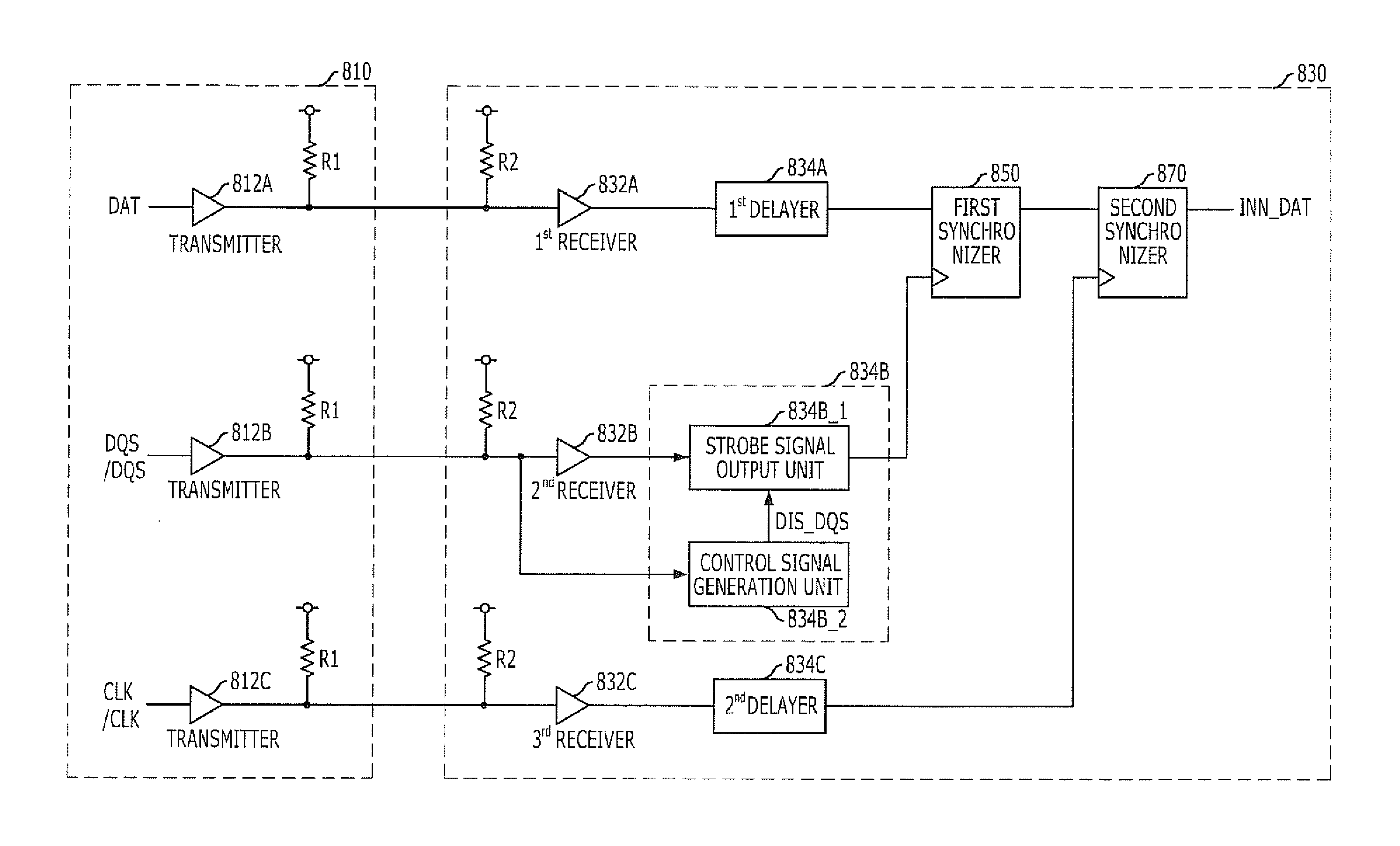
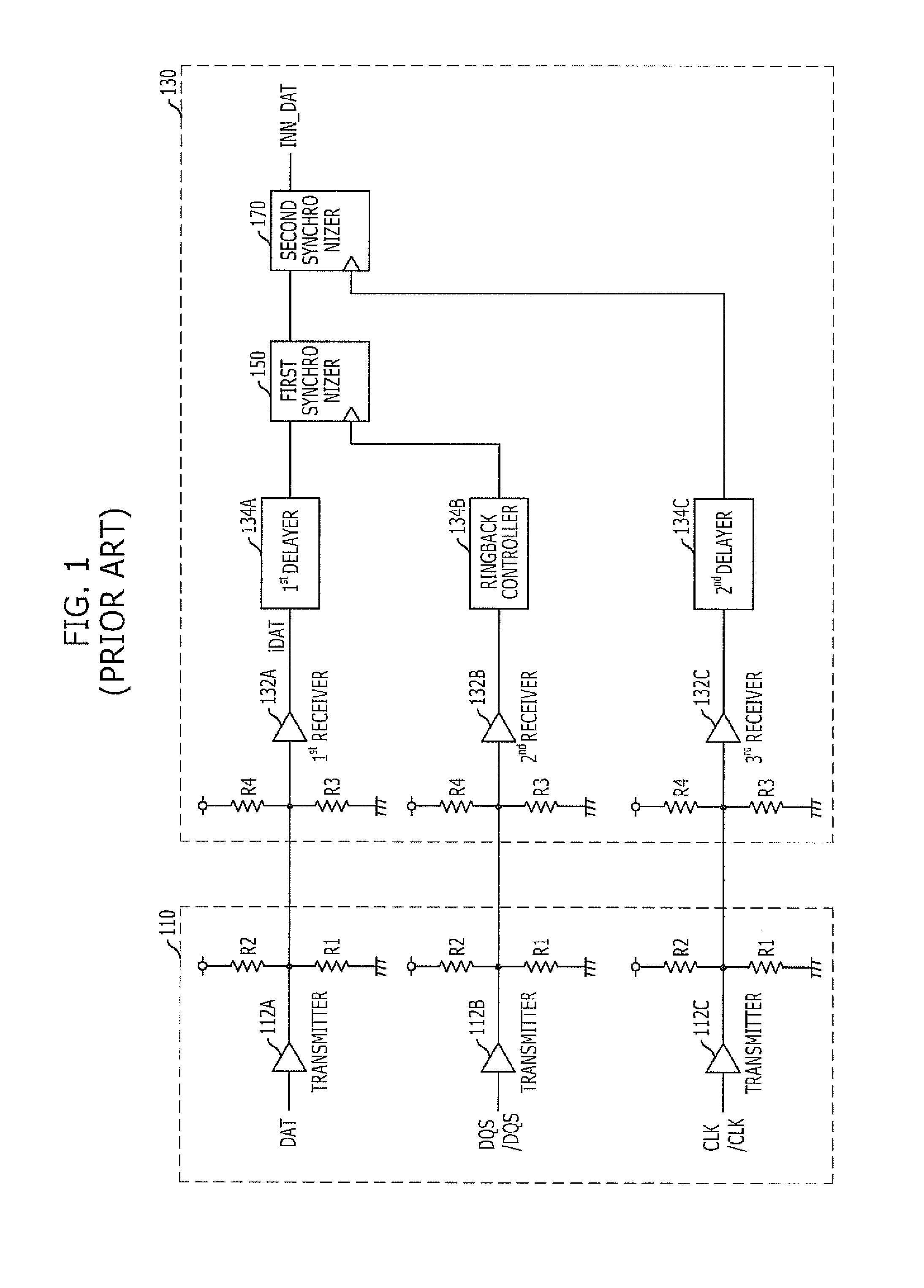
[0042]FIG. 8 is a block diagram illustrating a system structure in accordance with an embodiment of the present invention. Referring to FIG. 8, a system includes a chipset 810 and a semiconductor memory device 830. The chipset 810 outputs a data DAT, a first data strobe signal DQS, a second data strobe signal / DQS, which is an inverted signal of the first data strobe signal DQS, a first external clock signal CLK, and a second external clock signal / CLK, which is an inverted signal of the first external clock signal CLK, to the semiconductor memory device 830. Herein, the data DAT, the first and second data strobe signals DQS and / DQS, and the first and second external clock signal CLK and / CLK are outputted through first to third transmitters 812A, 812B and 812C, respectively.
[0043]The signals outpu...
PUM
 Abstract
Description
Claims
Application Information
 - R&D
- Intellectual Property
- Life Sciences
- Materials
- Tech Scout
- Unparalleled Data Quality
- Higher Quality Content
- 60% Fewer Hallucinations
Browse by: Latest US Patents, China's latest patents, Technical Efficacy Thesaurus, Application Domain, Technology Topic, Popular Technical Reports.
© 2025 PatSnap. All rights reserved.Legal|Privacy policy|Modern Slavery Act Transparency Statement|Sitemap|About US| Contact US: help@patsnap.com