Transverse Force, Pressure and Vibration Sensors using Piezoelectric Nanostructures

Inactive Publication Date: 2011-01-13
GEORGIA TECH RES CORP
View PDF41 Cites 24 Cited by
  • Summary
  • Abstract
  • Description
  • Claims
  • Application Information

AI Technical Summary

Benefits of technology

[0011]In another aspect, the invention is a gated electrical device that includes an elongated piezoelectric semiconducting nanostructure, a first electrode, a second electrode, an insulative material and a bias voltage source. The elongated piezoelectric semiconducting nanostructure includes a first portion and a second portion contiguous thereto. The first electrode is electrically coupled to a first end of the first portion of the elongated piezoelectric semiconducting nanostructure. The second electrode is electrically coupled to a second end, spaced apart from the first end, of the first portion of the elongated piezoelectric semiconducting nanostructure. The insulative material covers the first portion of the elongated piezoelectric semiconducting nanostructur

Problems solved by technology

This type of configuration may not be advantageous for fabricating devices that simulate the action of hairy beams (su

Method used


Image

  • Transverse Force, Pressure and Vibration Sensors using Piezoelectric Nanostructures
  • Transverse Force, Pressure and Vibration Sensors using Piezoelectric Nanostructures
  • Transverse Force, Pressure and Vibration Sensors using Piezoelectric Nanostructures

Examples


Embodiment Construction

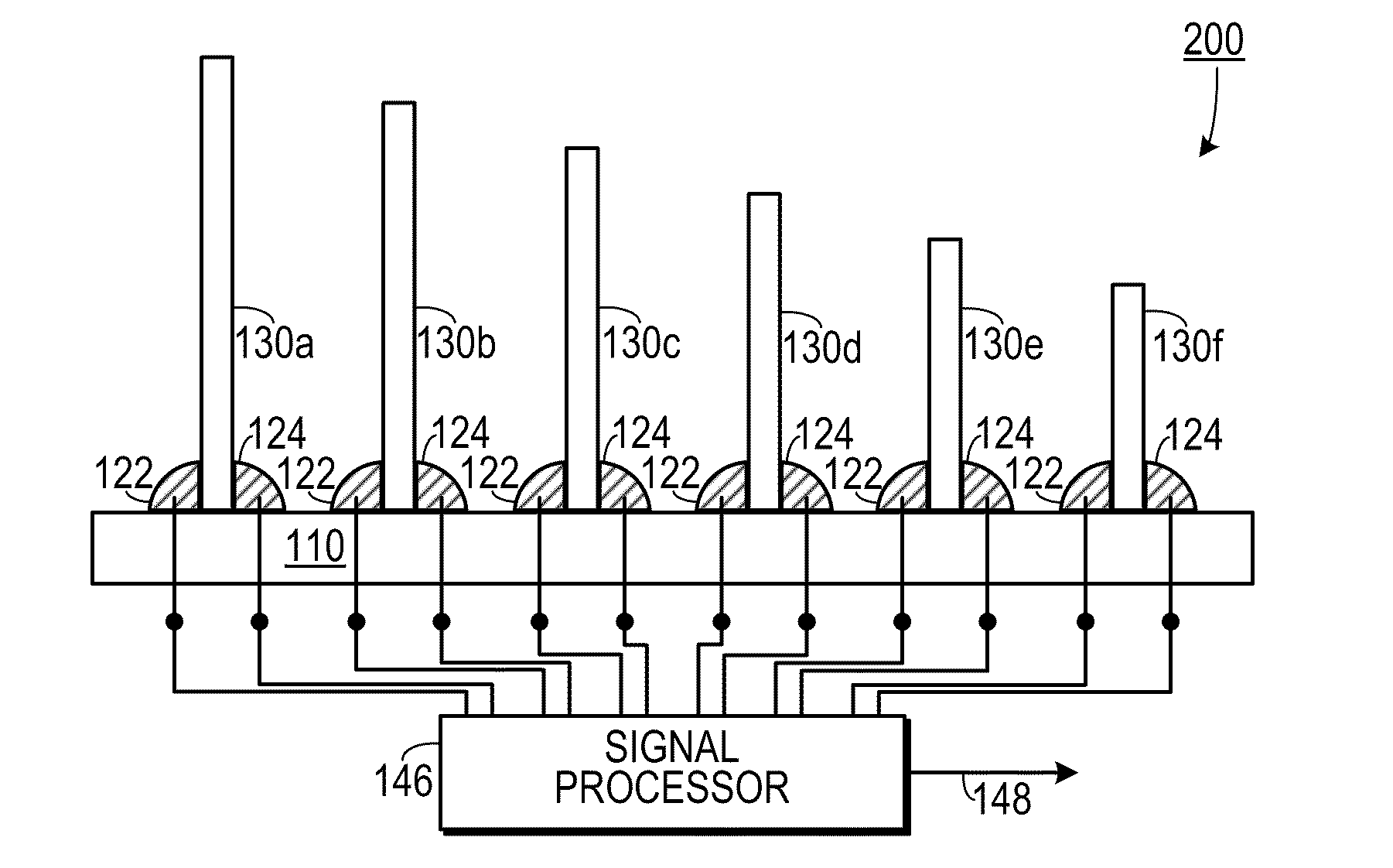
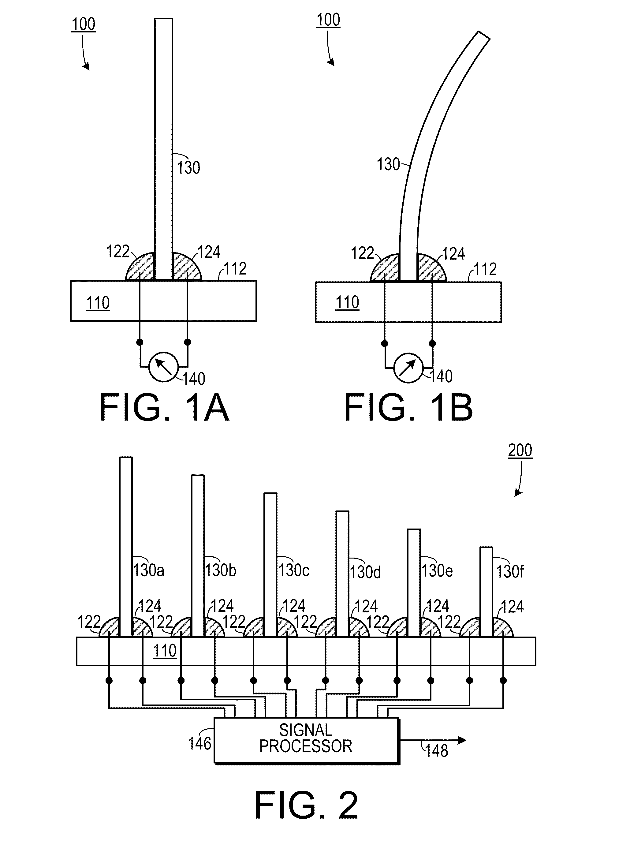
[0022]A preferred embodiment of the invention is now described in detail. Referring to the drawings, like numbers indicate like parts throughout the views. Unless otherwise specifically indicated in the disclosure that follows, the drawings are not necessarily drawn to scale. As used in the description herein and throughout the claims, the following terms take the meanings explicitly associated herein, unless the context clearly dictates otherwise: the meaning of “a,”“an,” and “the” includes plural reference, the meaning of “in” includes “in” and “on.” Also as used herein, “fine nanowire” means a structure having a diameter of less than 5 μm and a length of at least 23 μm.

[0023]U.S. Pat. Nos. 6,586,095 and 7,220,310 (both issued to Wang et al.) disclose methods of making nanowires that may be used in the embodiments disclosed below and, therefore, these patents are incorporated herein by reference.

[0024]In one embodiment, the invention is a vibration sensor employing at least one pi...


PUM


Abstract

An electrical device includes an insulating substrate; an elongated piezoelectric semiconductor structure, a first electrode and a second electrode. A first portion of the elongated piezoelectric semiconductor structure is affixed to the substrate and a second portion of the elongated piezoelectric semiconductor structure extends outwardly from the substrate. The first electrode is electrically coupled to a first end of the first portion of the elongated piezoelectric semiconductor structure. The second electrode is electrically coupled to a second end of the first portion of the elongated piezoelectric semiconductor structure.

Description

CROSS-REFERENCE TO RELATED APPLICATION(S)[0001]This application claims the benefit of U.S. Provisional Patent Application Ser. No. 61 / 234,009, filed Aug. 14, 2009, the entirety of which is hereby incorporated herein by reference.[0002]This application is a continuation-in-part of, and claims the benefit of, U.S. patent application Ser. No. 12 / 202,849, filed Sep. 2, 2008, the entirety of which is hereby incorporated herein by reference.STATEMENT OF GOVERNMENT INTEREST[0003]This invention was made with government support under contract No. W31P4Q-08-1-0009, awarded by the U.S. Army. The government has certain rights in the invention.BACKGROUND OF THE INVENTION[0004]1. Field of the Invention[0005]The present invention relates to gated electronic devices and, more specifically, to a gated electronic device that includes a nanoscale piezoelectric gating mechanism.[0006]2. Description of the Related Art[0007]One-dimensional (1D) nano-materials have profound applications in biological and ...

Claims


Application Information

Patent Timeline
IPC IPC(8): H01L29/84H01L41/047H01L41/113H01L21/44
CPCH04R17/02H04R25/60H04R31/006H01L29/413H01L29/775H01L29/84H01L29/0676B82Y10/00H04R25/603H04R25/609
Inventor WANG, ZHONG L.FEI, PENG
Owner GEORGIA TECH RES CORP
Why Eureka
Try Eureka