Chip package and manufacturing method thereof

a technology of chip and manufacturing method, applied in the field of semiconductor devices, can solve the problems of serious and challenging problems of electronic devices or systems, such as electromagnetic interference, and achieve the effect of less effort and better design flexibility

Active Publication Date: 2011-01-13
ADVANCED SEMICON ENG INC
View PDF32 Cites 108 Cited by
  • Summary
  • Abstract
  • Description
  • Claims
  • Application Information

AI Technical Summary

Benefits of technology

[0006]In view of the foregoing, the present invention provides a manufacturing method of a chip package, which offers better design flexibility with less effort.
[0007]The present invention is further directed to a chip package with enhanced effectiveness of EMI shielding.
[0012]According to the embodiments of the present invention, the grinding process makes the top edges of the molding compound blunt or rounded, so that the later formed shielding layer can smoothly covers the top edges or corners of the molding compound of individual chip packages, without the crevices.
[0013]Herein, the crevices often occurring at the orthogonal corners or edges of the shielding layer can be avoided, and the shielding layer can uniformly cover the molding compound of the chip package and provide effective EMI shield of the chip package. According to the present invention, owing to the complete coverage of the shielding layer, the reliability of the package and the shielding efficacy can be improved.

Problems solved by technology

Electro-magnetic interference (EMI) is a serious and challenging problem for most electronic devices or systems.
Conventionally, EMI shielding solutions typically involve the use of metal plates and / or conductive gaskets, which are later attached or affixed at higher manufacturing costs.

Method used


Image

  • Chip package and manufacturing method thereof
  • Chip package and manufacturing method thereof
  • Chip package and manufacturing method thereof

Examples


Embodiment Construction

[0020]Reference will now be made in detail to the present preferred embodiments of the invention, examples of which are illustrated in the accompanying drawings. Wherever possible, the same reference numbers are used in the drawings and the description to refer to the same or like parts.

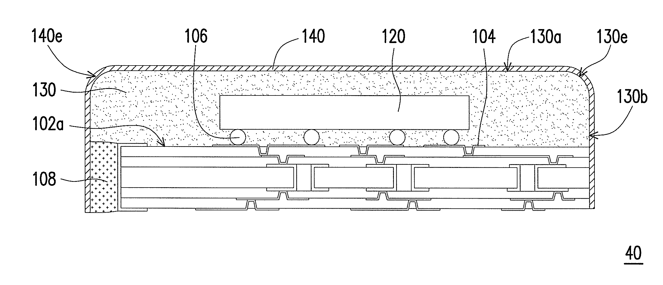
[0021]The manufacturing methods as described in the present invention can be used for fabricating various package structures and are more suitable for fabricating stacked type packages, multiple-chip packages, or high frequency device packages (including radio frequency device packages).

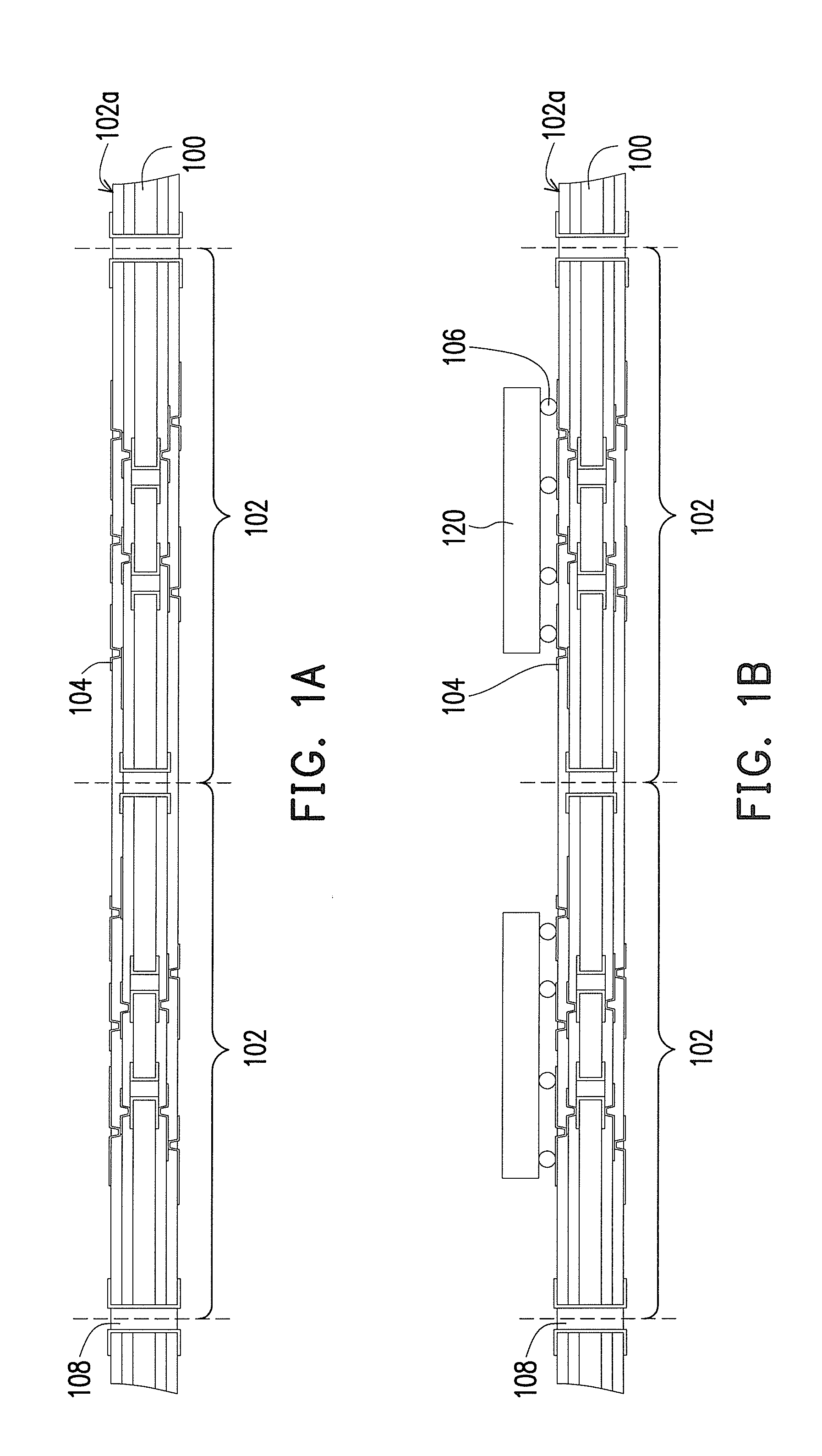
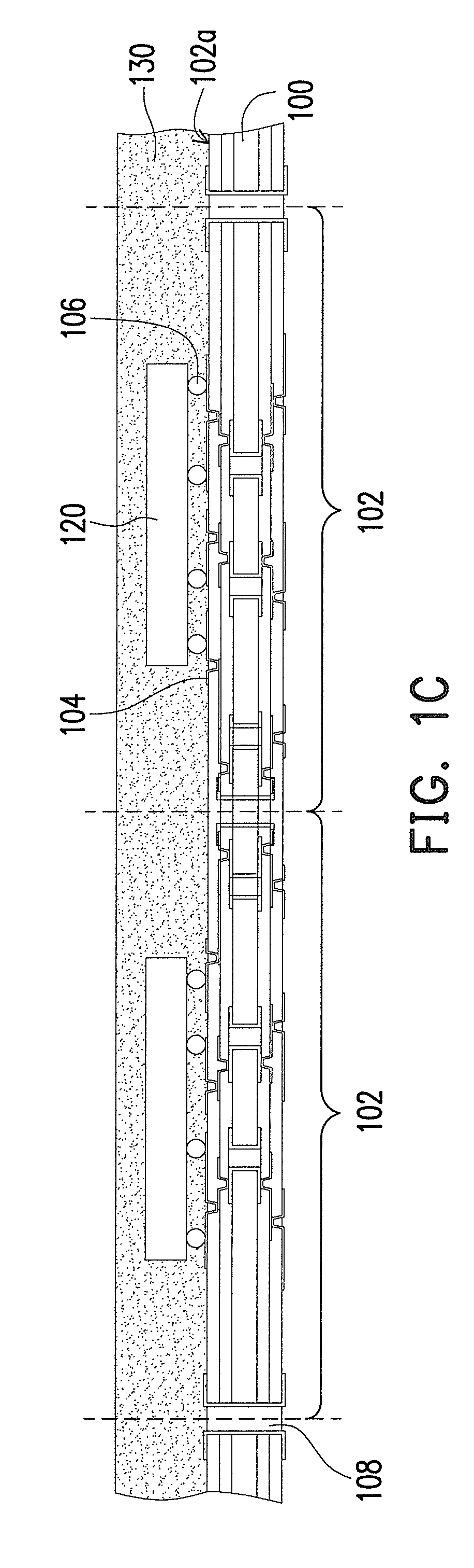
[0022]FIGS. 1A through 1G are schematic views showing a manufacturing method of the chip package according to the preferred embodiment of the present invention. FIG. 1D′ and 1D″ are exemplary three-dimensional schematic views showing the structure of FIG. 1D having grinding trenches of enlarged view A or B.

[0023]Referring to FIG. 1A, a matrix substrate 100 having a plurality of substrate 102 (defined by the subsequent...


PUM


Abstract

A chip package including a shielding layer conformally covering the underlying molding compound for is provided. The shielding layer can smoothly cover the molding compound and over the rounded or blunted, top edges of the molding compound, which provides better electromagnetic interferences shielding and better shielding performance.

Description

BACKGROUND OF THE INVENTION[0001]1. Field of the Invention[0002]The present invention relates to a semiconductor device, and more particularly to a chip package.[0003]2. Description of Related Art[0004]Electro-magnetic interference (EMI) is a serious and challenging problem for most electronic devices or systems. As EMI disturbances commonly interrupt, degrade or limit the effective performance of the electronic device or the whole circuit of the electronic system, it is necessary for the electronic devices or systems to have efficient EMI protection to ensure the effective and safe operation.[0005]EMI protection is particularly important in small-sized, densely packaged or sensitive electronic applications operating at high frequencies. Conventionally, EMI shielding solutions typically involve the use of metal plates and / or conductive gaskets, which are later attached or affixed at higher manufacturing costs.SUMMARY OF THE INVENTION[0006]In view of the foregoing, the present invent...

Claims


Application Information

Patent Timeline
Patent Type & Authority Applications(United States)
IPC IPC(8): H01L23/552H01L21/78
CPCH01L21/561H01L2924/014H01L23/3121H01L23/49805H01L23/49822H01L23/552H01L24/16H01L24/97H01L2224/16225H01L2224/97H01L2924/01013H01L2924/01029H01L2924/01033H01L2924/01047H01L2924/01078H01L2924/01079H01L2924/1815H01L2924/3025H01L21/565H01L2924/01024H01L2924/01005H01L2924/01006H01L2224/81H01L2924/181H01L2924/00012
Inventor LIAO, KUO-HSIEN
Owner ADVANCED SEMICON ENG INC
Why Eureka
Try Eureka