
High current control circuit including metal-insulator transition device, and system including the high current control circuit

a technology of high current control and transition device, which is applied in the direction of process and machine control, pulse technique, instruments, etc., can solve the problems of large size, high packaging cost of power semiconductor transistors, and difficulty in switching a high current by using semiconductor transistors

Inactive Publication Date: 2011-01-13
ELECTRONICS & TELECOMM RES INST
View PDF6 Cites 5 Cited by
  • Summary
  • Abstract
  • Description
  • Claims
  • Application Information

AI Technical Summary

Benefits of technology

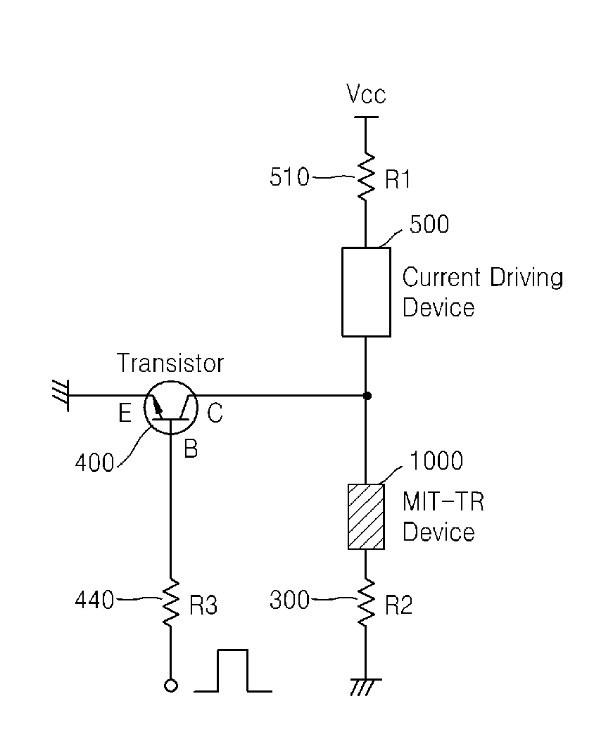
[0010]The present invention provides a high current control circuit including a metal-insulator transition (MIT) device, and a system including the high current control circuit so that a high current can be controlled and switched by the small-size high current control circuit, and thus, a heat generation problem caused in a conventional semiconductor transistor, as described above, can be solved.
[0013]When the heat-preventing transistor is the bipolar transistor, a first electrode of the MIT device, a second electrode of the MIT device, an emitter electrode of the bipolar transistor may be respectively connected to a collector electrode of the bipolar transistor, a base electrode of the bipolar transistor, and ground, and the first electrode of the MIT device and the collector electrode of the bipolar transistor may be connected to the current driving device and the switching control transistor, and the second electrode of the MIT device and the base electrode of the bipolar transistor may be connected to ground via a MIT resistor for protection of the MIT device.
[0014]When the heat-preventing transistor is the MOS transistor, a first electrode of the MIT device, a second electrode of the MIT device, and a source electrode of the MOS transistor may be respectively connected to a drain electrode of the MOS transistor, a gate electrode of the MOS transistor, and ground, and the first electrode of the MIT device and the drain electrode of the MOS transistor may be connected to the current driving device and the switching control transistor, and the second electrode of the MIT device and the gate electrode of the MOS transistor may be connected to ground via a MIT resistor for protection of the MIT device.
[0021]The secondary cell may be a lithium ion cell, the MIT device may undergo the abrupt MIT at a predetermined critical temperature or higher, and when a temperature of the lithium ion cell exceeds the predetermined critical temperature, the MIT-TR composite device may discharge charges of the lithium ion cell to prevent explosion of the lithium ion cell.
[0023]The MIT device may undergo an abrupt MIT at a critical temperature or higher, the PTC device may block a current at the critical temperature, and when a temperature of the secondary cell exceeds the critical temperature, the PTC device may block a current supply to the current driving system, and the MIT-TR composite device may discharge charges of the secondary cell, whereby explosion of the secondary cell may be prevented.

Problems solved by technology

However, in general, semiconductors have a current density of about 102 to about 104 A / cm2, thus, it is difficult to switch a high current by using semiconductor transistors.
Thus, the power semiconductor transistors incur high packaging costs due to the high-temperature heat problem, and have large sizes due to the inclusion of the heat radiation plate, etc.
As a result, electric and electronic systems using such power semiconductor transistors are obliged to have large sizes due to the large sizes of the power semiconductor transistors, and also incur high costs.

Method used


Image

  • High current control circuit including metal-insulator transition device, and system including the high current control circuit
  • High current control circuit including metal-insulator transition device, and system including the high current control circuit
  • High current control circuit including metal-insulator transition device, and system including the high current control circuit

Examples


Embodiment Construction

[0037]The present invention will now be described more fully with reference to the accompanying drawings, in which exemplary embodiments of the invention are shown. Throughout the specification, it will be understood that when an element is referred to as being “on” another element, it can be directly on the other element, or intervening elements may also be present. In the drawings, the thicknesses of layers and regions are exaggerated for clarity. Like reference numerals in the drawings denote like elements, and thus their description will be omitted. Meanwhile, it will be understood by those of ordinary skill in the art that terms in the present invention are used therein without departing from the spirit and scope of the present invention as defined by the following claims. In the following description, well-known functions or constructions are not described in detail since they would obscure the invention with unnecessary detail.

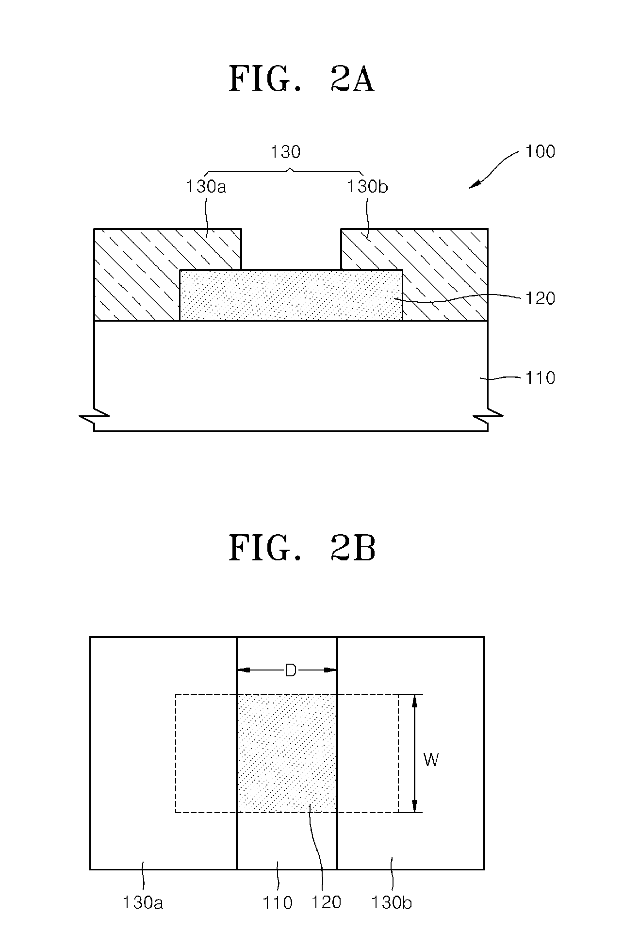
[0038]FIGS. 2A and 2B respectively correspond to ...


PUM


Abstract

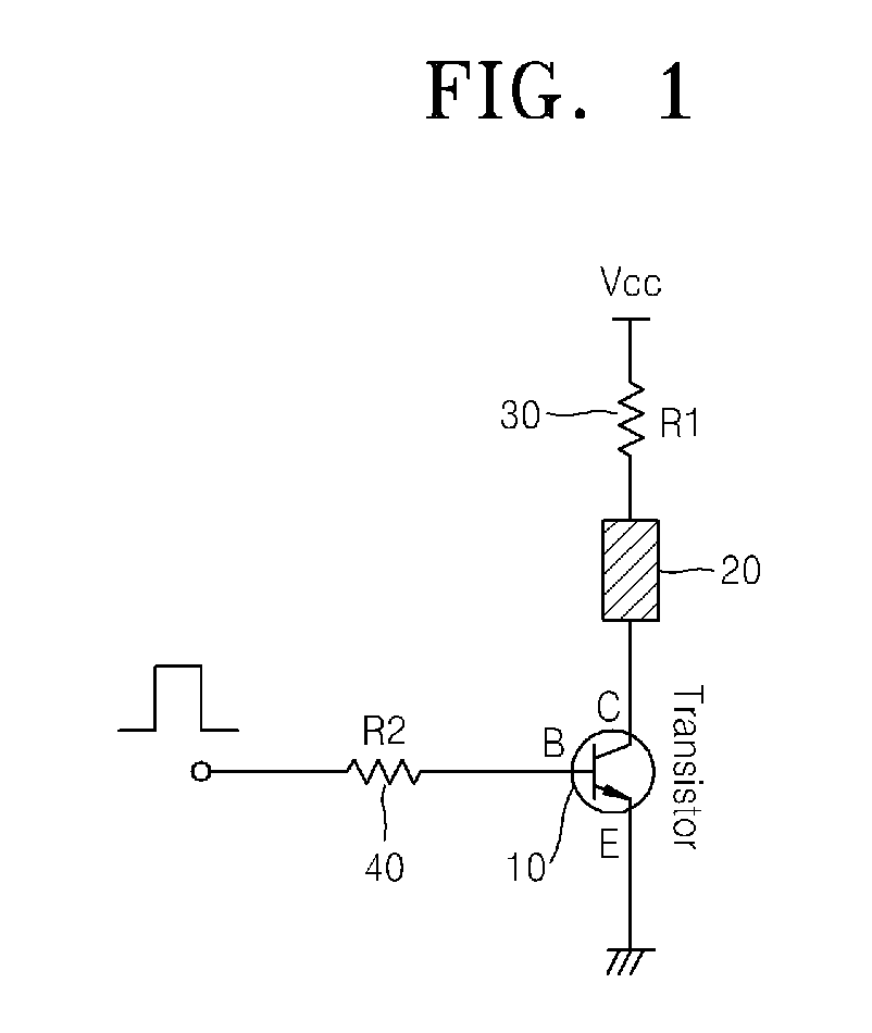
Provided are a high current control circuit including a metal-insulator transition (MIT) device, and a system including the high current control circuit so that a high current can be controlled and switched by the small-size high current control circuit, and a heat generation problem can be solved. The high current control circuit includes the MIT device connected to a current driving device and undergoing an abrupt MIT at a predetermined transition voltage; and a switching control transistor connected between the current driving device and the MIT device and controlling on-off switching of the MIT device. By including the metal-insulator transition (MIT) device, the high current control circuit switches a high current that is input to or output from the current driving device. Also, the MIT device constitutes a MIT-TR composite device with a heat-preventing transistor which prevents heat generation and is connected to the MIT device.

Description

CROSS-REFERENCE TO RELATED PATENT APPLICATION[0001]This application claims the benefit of Korean Patent Application Nos. 10-2008-0018557, filed on Feb. 28, 2008, and 10-2008-0091266, filed on Sep. 17, 2008 in the Korean Intellectual Property Office, the disclosures of which are incorporated herein their entirety by reference.BACKGROUND OF THE INVENTION[0002]1. Field of the Invention[0003]The present invention relates to a metal-insulator transition (MIT) device, and more particularly, to a circuit including the MIT device, capable of controlling a high current with low temperature heat in that high-temperature heat is generated in a transistor when a high current flows through the transistor.[0004]2. Description of the Related Art[0005]Conventionally, in order to control and switch a high current, e.g., a current having a current density of about 106 A / cm2, power semiconductor transistors have been used. However, in general, semiconductors have a current density of about 102 to abou...

Claims


Application Information

Patent Timeline
IPC IPC(8): H03K17/60
CPCH01L21/8222H01L27/067H01L27/082H01L49/003H01L23/62H01L2924/0002H03K17/14H03K17/567H01L2924/00G05F3/24
Inventor KIM, HYUN-TAKKIM, BONG-JUNYUN, SUN-JIN
Owner ELECTRONICS & TELECOMM RES INST
Learn More