Peak factor reduction device and base station
- Summary
- Abstract
- Description
- Claims
- Application Information
AI Technical Summary
Benefits of technology
Problems solved by technology
Method used
Image
Examples
first embodiment
[0044]A first embodiment will be explained with reference to FIGS. 3 through 9. In FIG. 3, a peak factor reduction device 100A includes a peak detection circuit 101, a threshold value comparison circuit 102, an NCO 103, a delayer 104, two delayers 105, a filter (FIL) circuit 107, a power calculation circuit 111, an integrator 112, a plurality of adders, and a plurality of multipliers. Inputs to the peak factor reduction device 100A include an input signal, a detection width, an EVM target value, and a PFR initial threshold value. The input signal is of a complex signal having I and Q components. An output of the peak factor reduction device 100A is of an output signal reduced in peak factor. Incidentally, double lines defined between blocks in the following drawings mean plural signals respectively.
[0045]Firstly, the peak factor reduction device 100A multiplies complex base band signals of at least one or more carriers each having a uniform spectrum by complex exponential functions ...
second embodiment
[0063]A second embodiment will next be explained with reference to FIGS. 10 through 12. When the peak limit is incomplete and the error component remains as a result of offsetting of the peak factors in the peak factor reduction circuit, the peak factor reduction devices have heretofore been stacked in multistage in the patent document 1. When such a configuration is taken, the logic scale as for each peak factor reduction device increases.
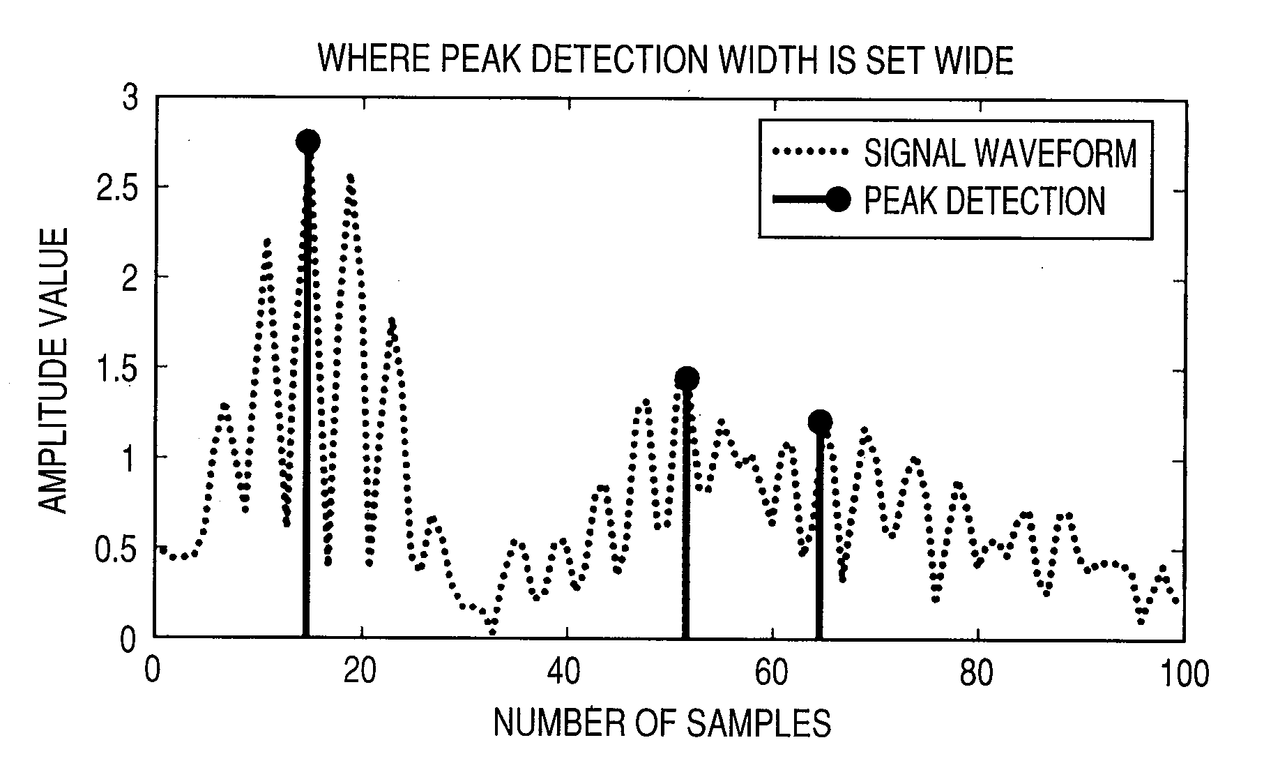
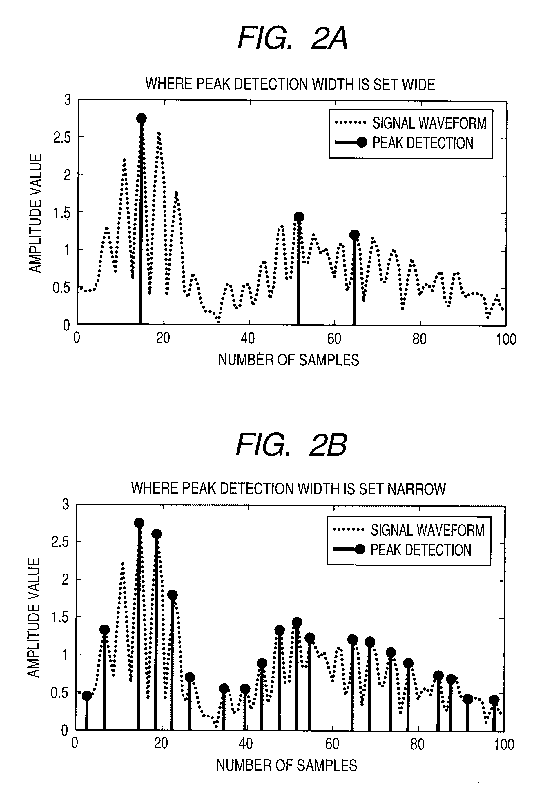
[0064]A function for automatically adjusting a peak detection width at a peak factor reduction device 100B will therefore be described while referring to FIG. 10. Making this adjustment effective enables reducing the remaining or residual probability of an error component at the offsetting of peak factors. A peak factor reduction technique is similar to that according to the first embodiment. In FIG. 10, the peak factor reduction device 100B includes a peak detection circuit 101, a threshold value comparison circuit 102, an NCO 103, a delayer 104,...
third embodiment
[0072]A third embodiment will next be explained with reference to FIG. 13. In FIG. 13, a peak factor reduction device 100C includes a peak detection circuit 101, a threshold value comparison circuit 102, an NCO 103, a delayer 104, two delayers 105, a FIL circuit 107, a power calculation circuit 111, an integrator 112, an amplitude comparison circuit 114, a plurality of adders and a plurality of multipliers. Inputs to the peak factor reduction device 100C include an input signal, an EVM target value, and a PFR initial threshold value. The input signal is of a complex signal having I and Q components. An output of the peak factor reduction device 100C is of an output signal reduced in peak factor.
[0073]The peak factor reduction device 100C is of a peak factor reduction device in which two elements corresponding to the function of automatically calculating a peak factor threshold value Vt brought to optimal within the EVM target value and the function of automatically adjusting a peak ...
PUM
 Abstract
Description
Claims
Application Information


