Solar cell and method for manufacturing solar cell

Inactive Publication Date: 2011-01-20
SEIKO EPSON CORP
View PDF4 Cites 2 Cited by
  • Summary
  • Abstract
  • Description
  • Claims
  • Application Information

AI Technical Summary

Benefits of technology

[0025]According to this configuration, the second electrode layer is formed in the outermost peripheral portion of each cell, and a space is formed between the second electrode layer and the adjacent other cells. Specifically, non-generating regions that do not contribute to electrical generation are eli

Problems solved by technology

However, reserving such a wide area increases the size of non-generating regions that do

Method used


Image

  • Solar cell and method for manufacturing solar cell
  • Solar cell and method for manufacturing solar cell
  • Solar cell and method for manufacturing solar cell

Examples


modification 1

[0058

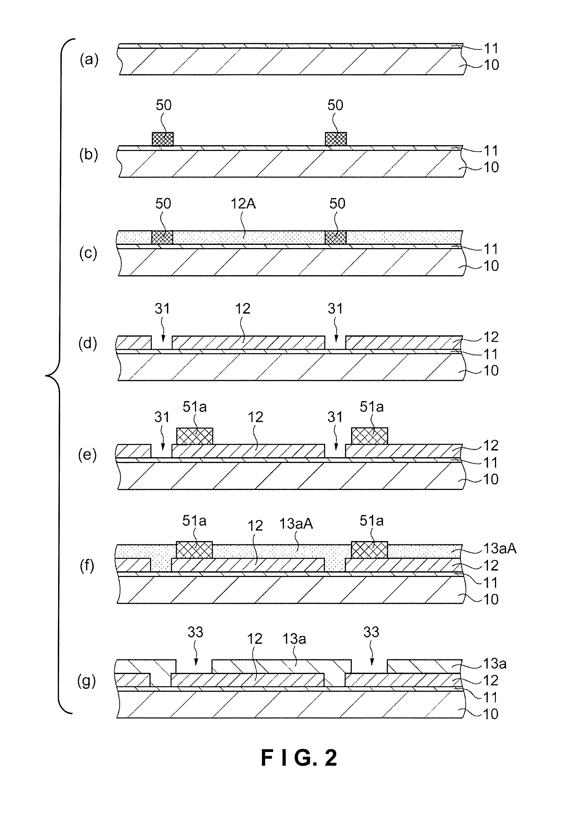
[0059]In the embodiment described above, the liquid material 12A including a first electrode material for forming the first electrode layer 12, as well as the other liquid materials, are applied using a printing method, an inkjet method, or another method, but this configuration is not limiting. For example, the liquid material 12A may be applied to the substrate 10 by a dipping method. Even when such a method is employed, because the partition portions 50 are fluid-repellent, the partition portions 50 repel the liquid material 12A, and the liquid material 12A can be applied in a predetermined region. A dipping method may be used to apply the other liquid materials 13aA, 13bA, and 14A as well.

modification 2

[0060

[0061]First through third partition portion formation steps are described in the embodiment above, but a configuration may also be adopted in which at least one partition portion formation step is performed, and the other partition portion formation steps are omitted. The scribing process can be eliminated in this configuration as well, and damage to other members can be reduced.

modification 3

[0062

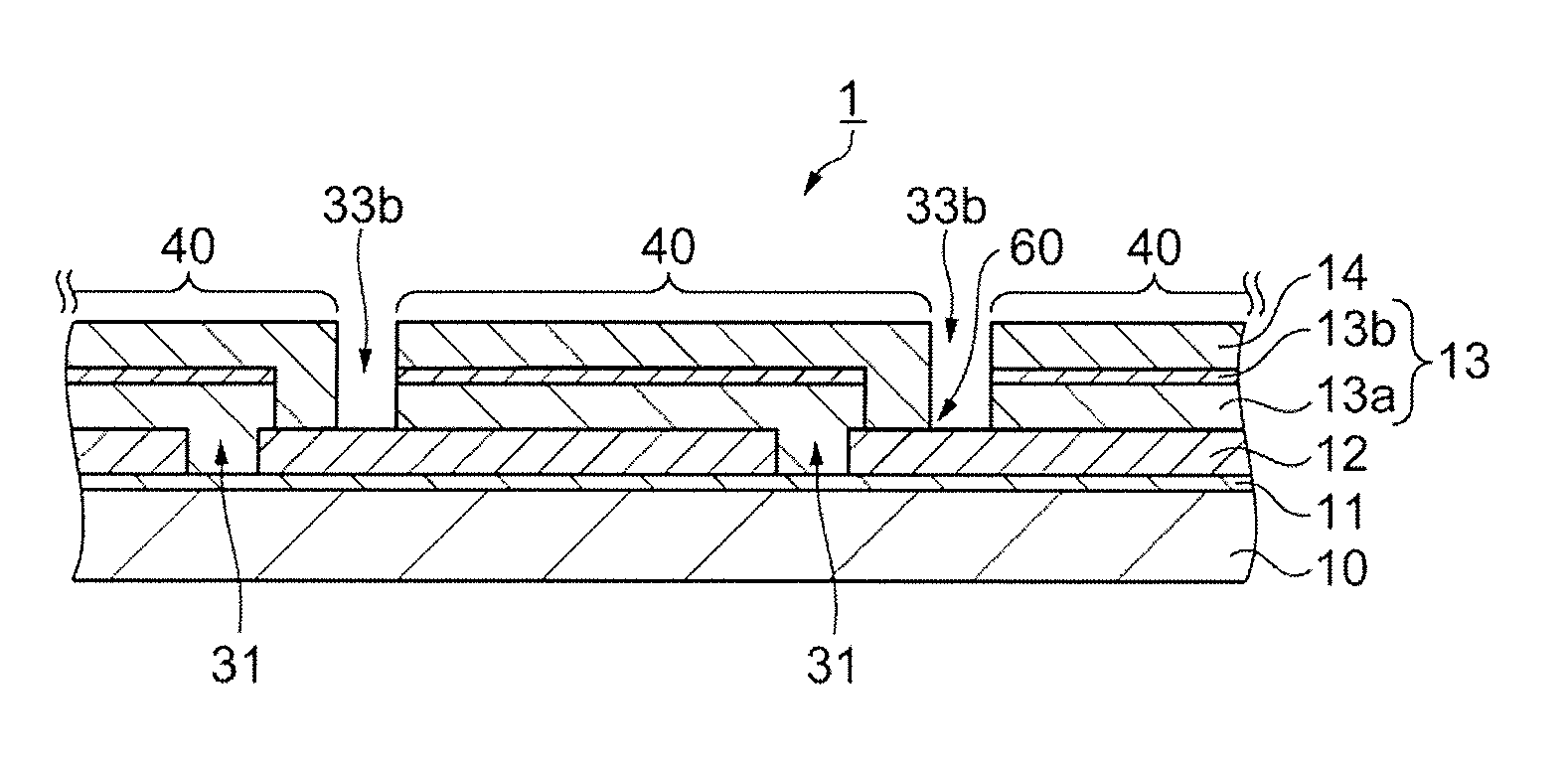
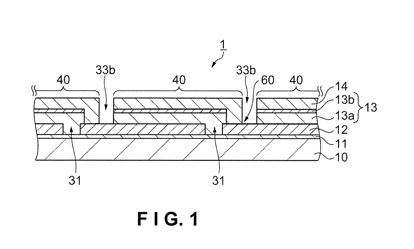
[0063]In the embodiment described above, a description is provided of the structure and other aspects of a CIGS-type solar cell 1, for receiving light from the side of the second electrode layer 14, but the solar cell 1, may also be a CIGS-type solar cell 1 that is capable of receiving light from the side of the substrate 10 as well as from the side of the second electrode layer 14. In this case, a transparent substrate is used as the substrate 10. For example, a glass substrate, a PET substrate, an organic transparent substrate, or the like may be used. Using a transparent substrate enables light to be received from the surface of the substrate 10. The first electrode layer 12 is a transparent electrode layer, and is a ZnOAl or other transparent electrode (TCO: transparent conducting oxides) layer, for example. By forming a transparent electrode layer, light that is incident from the side of the substrate 10 can be made to pass through to the semiconductor layer 13. The same e...


PUM


Abstract

A method is for manufacturing a solar cell having a plurality of unit cells connected in series, each of the unit cells including a substrate, a first electrode layer formed on the substrate, a semiconductor layer formed on the first electrode layer, and a second electrode layer formed on the semiconductor layer. The method includes forming a fluid-repellent partition portion on the substrate to partition a plurality of regions respectively corresponding to the first electrode layers of the unit cells, and applying a liquid material including a first electrode material for forming the first electrode layers on the regions of the substrate that are partitioned by the partition portion, and baking the applied liquid material to form the first electrode layers.

Description

CROSS-REFERENCE TO RELATED APPLICATIONS[0001]This application claims priority to Japanese Patent Application No. 2009-165345 filed on Jul. 14, 2009. The entire disclosure of Japanese Patent Application No. 2009-165345 is hereby incorporated herein by reference.BACKGROUND[0002]1. Technical Field[0003]The present invention relates to a solar cell and to a method for manufacturing a solar cell.[0004]2. Related Art[0005]A solar cell converts light energy into electrical energy, and various types of configurations of solar cells have been proposed according to the semiconductor used. In recent years, CIGS-type solar cells have been emphasized for the simple manufacturing process thereof and the ability to realize high conversion efficiency. A CIGS solar cell is configured from a plurality of unit cells connected in a series, where one cell is composed, for example, of a first electrode film formed on a substrate, a thin film that includes a compound semiconductor (copper-indium-gallium-s...

Claims


Application Information

Patent Timeline
IPC IPC(8): H01L31/0256H01L31/18
CPCY02E10/541H01L31/046H01L31/0749H01L31/022425H01L31/0463Y02P70/50
Inventor DENDA, ATSUSHISAITO, HIROMI
Owner SEIKO EPSON CORP
Why Eureka
Try Eureka