Electronic device mounting apparatus and resonance suppression method thereof

a technology for electronic devices and mounting apparatuses, which is applied in the direction of cooling/ventilation/heating modifications, semiconductor device details, semiconductor/solid-state device details, etc., can solve the problems of exceeding the allowable limit of electronic devices, and the short-circuit means of heat sink plates described in the patent document b>3/b> cannot be employed, so as to achieve the effect of deteriorating the heat discharge characteristics, excessively increasing the size of the heat sink plate, and without decreasing

Inactive Publication Date: 2009-11-12
NEC CORP
View PDF7 Cites 1 Cited by
  • Summary
  • Abstract
  • Description
  • Claims
  • Application Information

AI Technical Summary

Benefits of technology

[0015]In a present invention, a resonance suppressing member made of a dielectric material is mounted on a heat sink plate for extending an electric size to change the resonance frequency of the heat sink plate. Thus, without excessively increasing the size of the heat sink plate and without decreasing it to a degree deteriorating the heat discharge characteristics, the effective size of the heat sink plate can be made different from the half-wavelength size of the clock signal frequency transmitted through the electronic device or its harmonic frequencies. Hence, according to a present invention, it is possible to prevent the heat sink plate from resonance at the clock signal frequency of the electronic apparatus or its harmonic frequencies, and it is also possible to suppress the clock signal harmonic wave noise that is transmitted from the electronic apparatus to the heat sink plate and emitted from the heat sink plate.

Problems solved by technology

However, as disclosed in Japanese Laid-Open Patent-Application JP-P 2001-185893A, when an electric wave absorber is arranged between an electronic device and a heat discharging means, because of the thermal resistance of the radio wave absorber, the heat can not be discharged sufficiently from the heat discharging means, so that the temperature may exceed the allowable limit of the electronic device.
Further, when there is a constraint under which the heat sink plate cannot be connected to the circuit ground of the electronic device or the apparatus body ground, the short-circuit means of the heat sink plate described in the patent document 3 cannot be employed.

Method used


Image

  • Electronic device mounting apparatus and resonance suppression method thereof
  • Electronic device mounting apparatus and resonance suppression method thereof
  • Electronic device mounting apparatus and resonance suppression method thereof

Examples


first exemplary embodiment

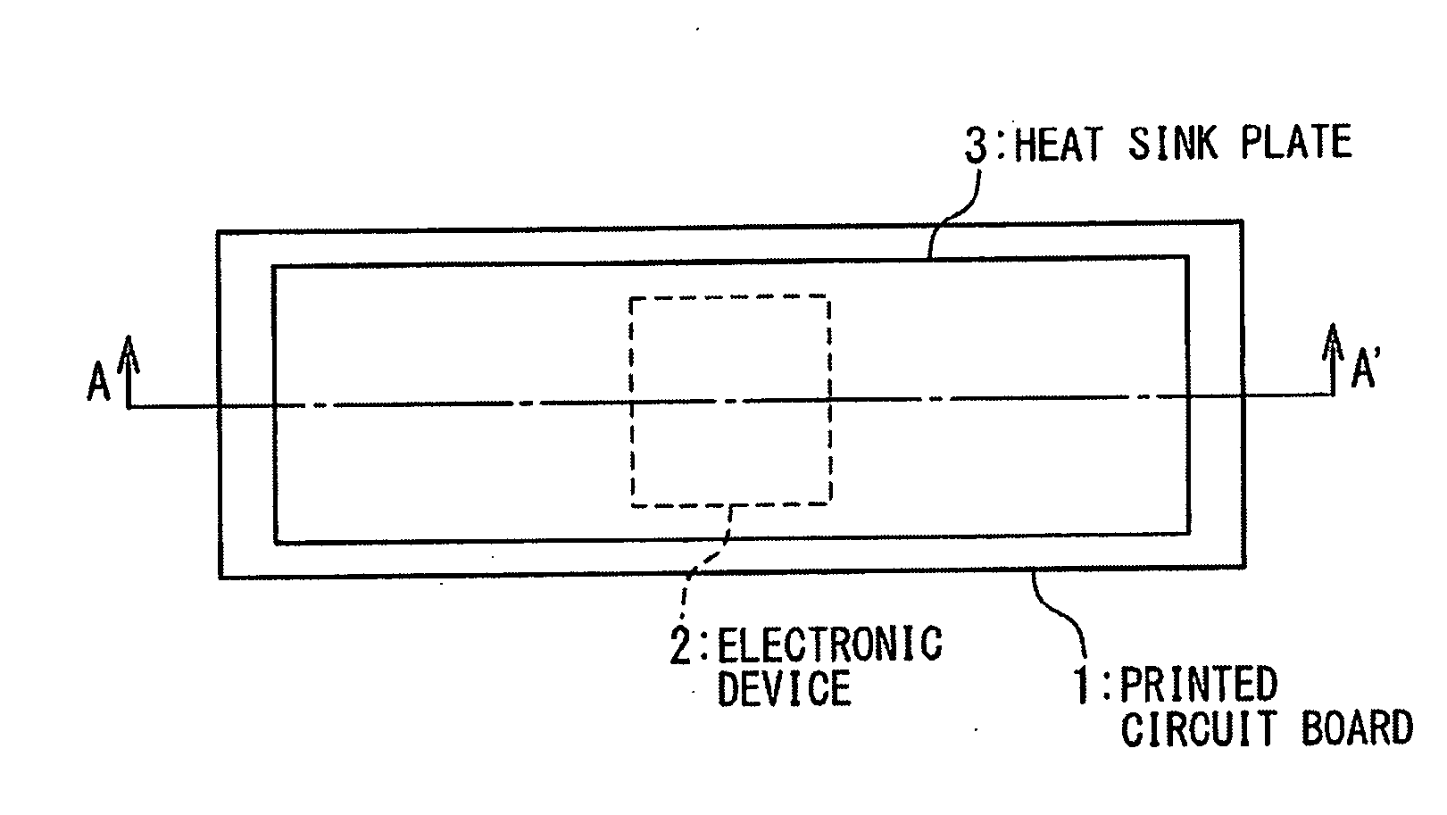
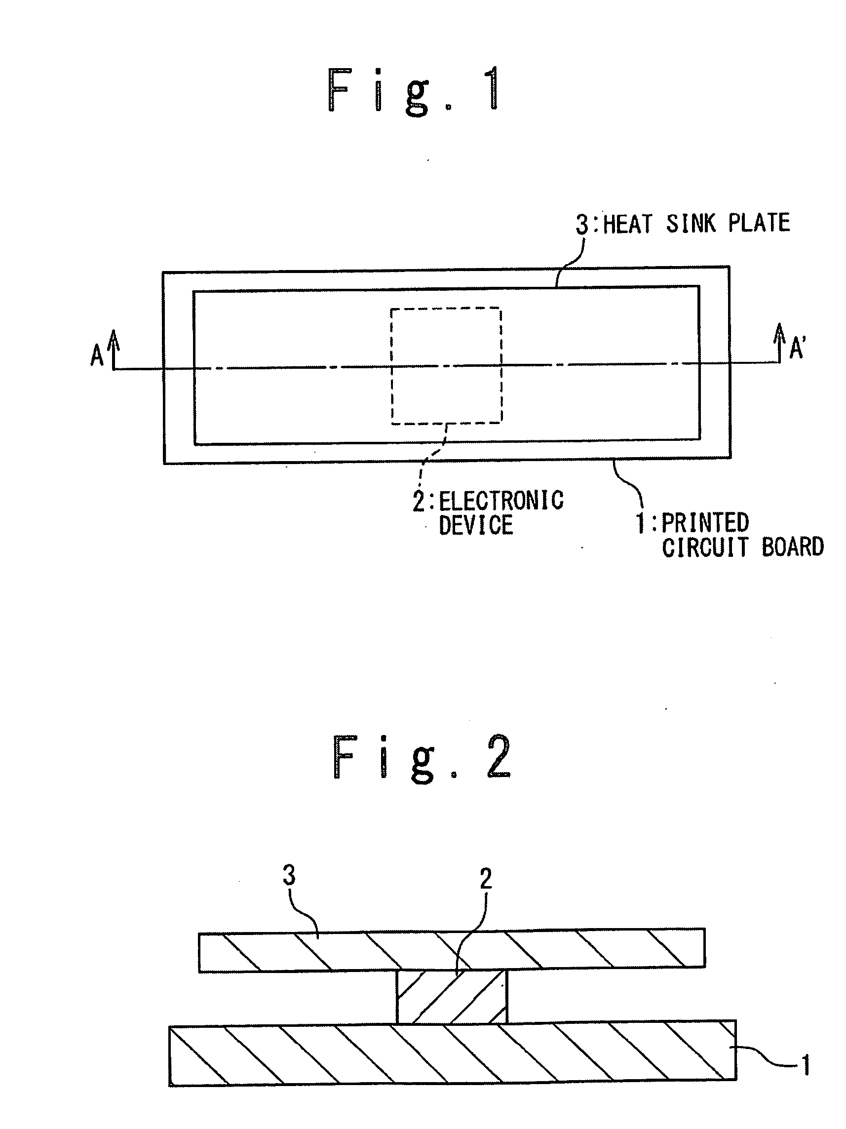
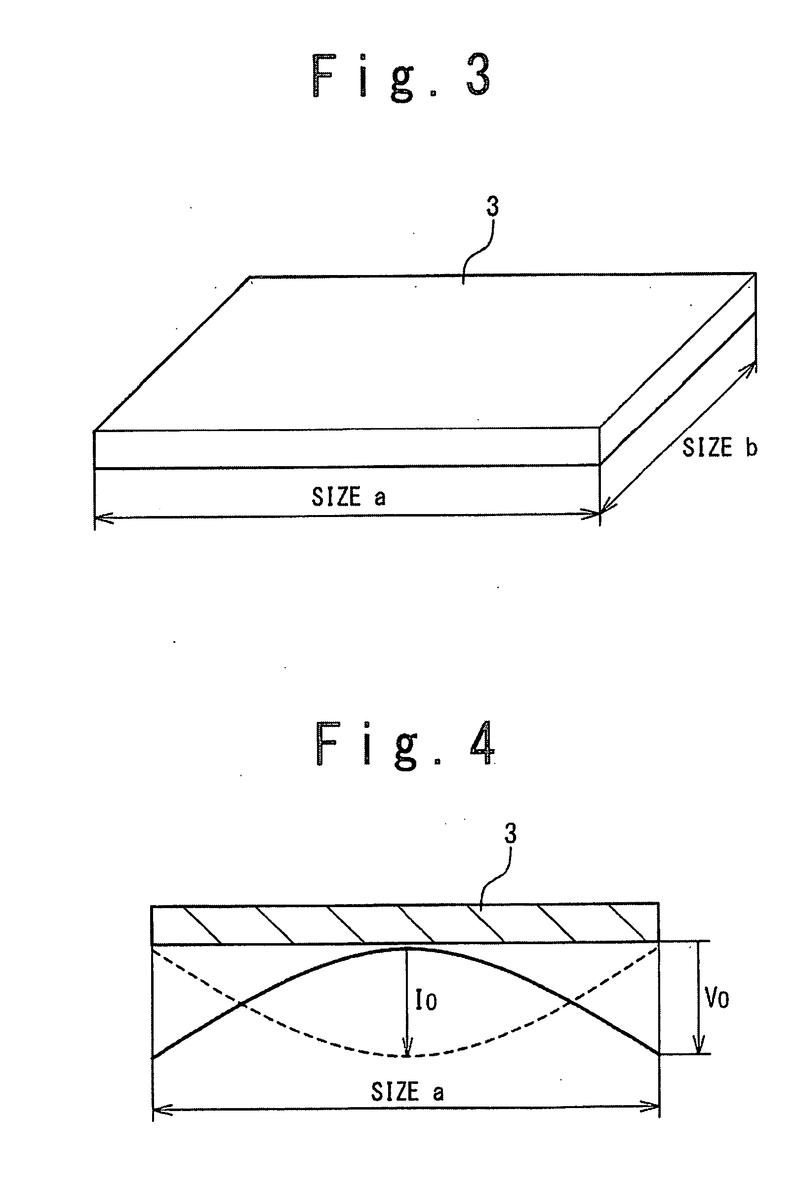
[0031]FIG. 5 is the top view of the electronic device mounting apparatus according to a first exemplary embodiment of a present invention, and FIG. 6 is the sectional view on the A-A′ line in FIG. 5. As shown in FIG. 5 and FIG. 6, the electronic device 2 is mounted on a printed circuit board 1. A heat sink plate 3 is placed on the electronic device 2, and dielectric strips 4, 5 made of dielectric material are mounted on both ends of the heat sink plate 3 on the side faced to the electronic device 2. The dielectric strips 4, 5 may be designed such that their dielectric constants are higher than 1 and metal may be included therein. As shown in FIG. 3, the size of one side of the heat sink plate 3 is represented by “a,” and the other side thereof is represented by “b.”

[0032]For mounting the dielectric strips 4, 5 on the heat sink plate 3, adhesive bonding, fastening by using a bolt and the like, and elastically pushing attachment in which a pushing means is used can be applied, however...

second exemplary embodiment

[0039]FIG. 11 is the top view of an electronic device mounting apparatus according to a second exemplary embodiment of a present invention in which a plurality of electronic apparatuses are mounted and FIG. 12 is the sectional view of the A-A′ line in FIG. 11. As shown in FIG. 11 and FIG. 12, the plurality of electronic apparatuses 2 are mounted on a printed circuit board 1. A heat sink plate 3 is placed on the electronic apparatuses 2, and the dielectric strips 4, 5 are mounted on both the ends of the heat sink plate 3 on the side faced to the electronic apparatuses 2.

[0040]The side view from a direction where the size “a” side of the heat sink plate to which the dielectric strips 4, 5 are mounted on is shown in FIG. 7, similarly to the case of a first exemplary embodiment. As shown in FIG. 7, the half-wavelength of the clock signal harmonic wave noise frequency and the size “a” of the heat sink plate 3 are coincident to each other. However, since the dielectric strips 4, 5 are att...

third exemplary embodiment

[0042]FIG. 13 is the top view of an electronic device mounting apparatus in which a dielectric strip according to a third exemplary embodiment of a present invention is mounted to only one end of the heat sink plate, and FIG. 14 is a sectional view on the A-A′ line in FIG. 9. As shown in FIG. 13 and FIG. 14, an electronic device 2 is mounted on a printed circuit board 1. A heat sink plate 3 is placed on the electronic apparatuses 2, and the dielectric strip 4 is mounted on one end of the heat sink plate 3 on the side faced to the electronic apparatuses 2.

[0043]Also in this exemplary embodiment, the half-wavelength of the clock signal harmonic wave noise frequency and the size of the heat sink plate 3 are coincident to each other. However, because of the dielectric strip mounted on one end of the heat sink plate 3, the electric size of the heat sink plate 3 is extended. As a result, the electric size of the heat sink plate placed on electronic apparatuses can be made different from t...


PUM


Abstract

A heat sink plate is mounted on an electronic device for heat radiation of the electronic device. When the fundamental wave or a harmonic wave of the clock signal of the electronic device is coincide with the size of the heat sink plate, the heat sink plate resonates and large clock signal harmonic wave noise is radiated. For suppressing the noise, a dielectric strip is mounted on an edge portion of the heat sink plate. By this dielectric strip, the resonance frequency of the heat sink plate varies so that the resonance can be suppressed.

Description

TECHNICAL FIELD[0001]The present invention relates to a technique for suppressing resonance of a heat sink plate of an electronic device.BACKGROUND ART[0002]An electronic device, such as an LSI and the like, which is used in information processing apparatuses such as a personal computer, a work station and the like and carries out functions like the main storage, control and calculation and is configured by a single chip, requires large electric current for achieving high speed processing. For avoiding phenomenon that the heat generated by the large current causes the temperature of the electronic device to exceed an allowable limit, a heat discharging means is installed.[0003]FIG. 1 is the top view of an electronic device mounting apparatus having a heat discharging means which is an example for explaining a present invention, and FIG. 2 is a sectional view of an A-A′ line in FIG. 1.[0004]As shown in FIG. 1 and FIG. 2, an electronic device 2 which generates a large amount of heat, ...

Claims


Application Information

Patent Timeline
Patent Type & Authority Applications(United States)
IPC IPC(8): H05K7/20
CPCH01L23/367H01L2924/0002H01L2924/00
Inventor IMAZATO, MASAHARU
Owner NEC CORP
Why Eureka
Try Eureka