Integrated circuit including a large number of identical elementary circuits powered in parallel

a technology of integrated circuits and elementary circuits, which is applied in the direction of solid-state devices, electrical apparatus, and reliability increasing modifications, etc., can solve the problems of large space requirements and large errors of tree structures, and achieve the effect of increasing the space requirements of structures

Inactive Publication Date: 2011-01-20
E2V SEMICON
View PDF7 Cites 0 Cited by
  • Summary
  • Abstract
  • Description
  • Claims
  • Application Information

AI Technical Summary

Benefits of technology

[0014]The invention proposes a solution to make the potential difference applied between the head and the foot of each of the juxtaposed elementary circuits more uniform without unreasonably increasing the space requirement of the structure.

Problems solved by technology

In these structures with a large number of identical elementary circuits that must all receive in parallel one and the same potential, whether it be a high power supply potential or a low power supply potential, or a reference potential, or a potential to be measured, a difficulty is encountered which is associated with the fact that the voltage-supply conductors do not have an infinite conductivity but a conductivity that is limited by technological factors; the identical elementary circuits each consume a current which flows in this voltage-supply conductor; a voltage drop occurs in this conductor in proportion to the current consumed by the elementary circuits so that the elementary circuits receive different voltages depending on whether they are placed closer to or further from an upstream end of the conductor.
Even if the elementary voltage drop is very low, the error becomes considerable when N reaches one or several hundreds.
But the space requirement that would result from such a tree structure is very large if there are several hundreds of circuits to be powered.

Method used


Image

  • Integrated circuit including a large number of identical elementary circuits powered in parallel
  • Integrated circuit including a large number of identical elementary circuits powered in parallel
  • Integrated circuit including a large number of identical elementary circuits powered in parallel

Examples


Embodiment Construction

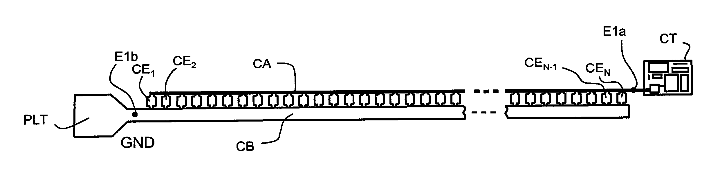
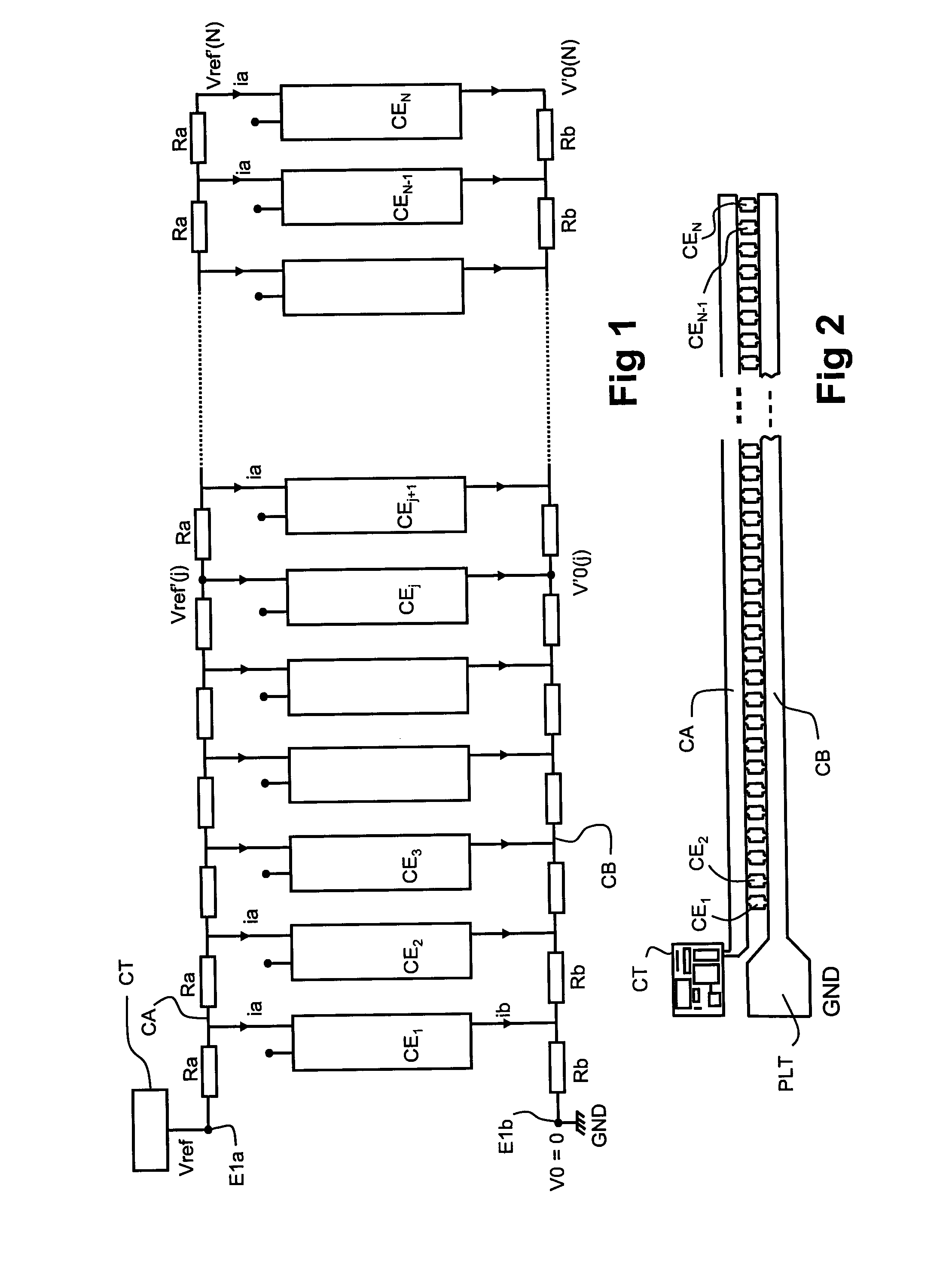
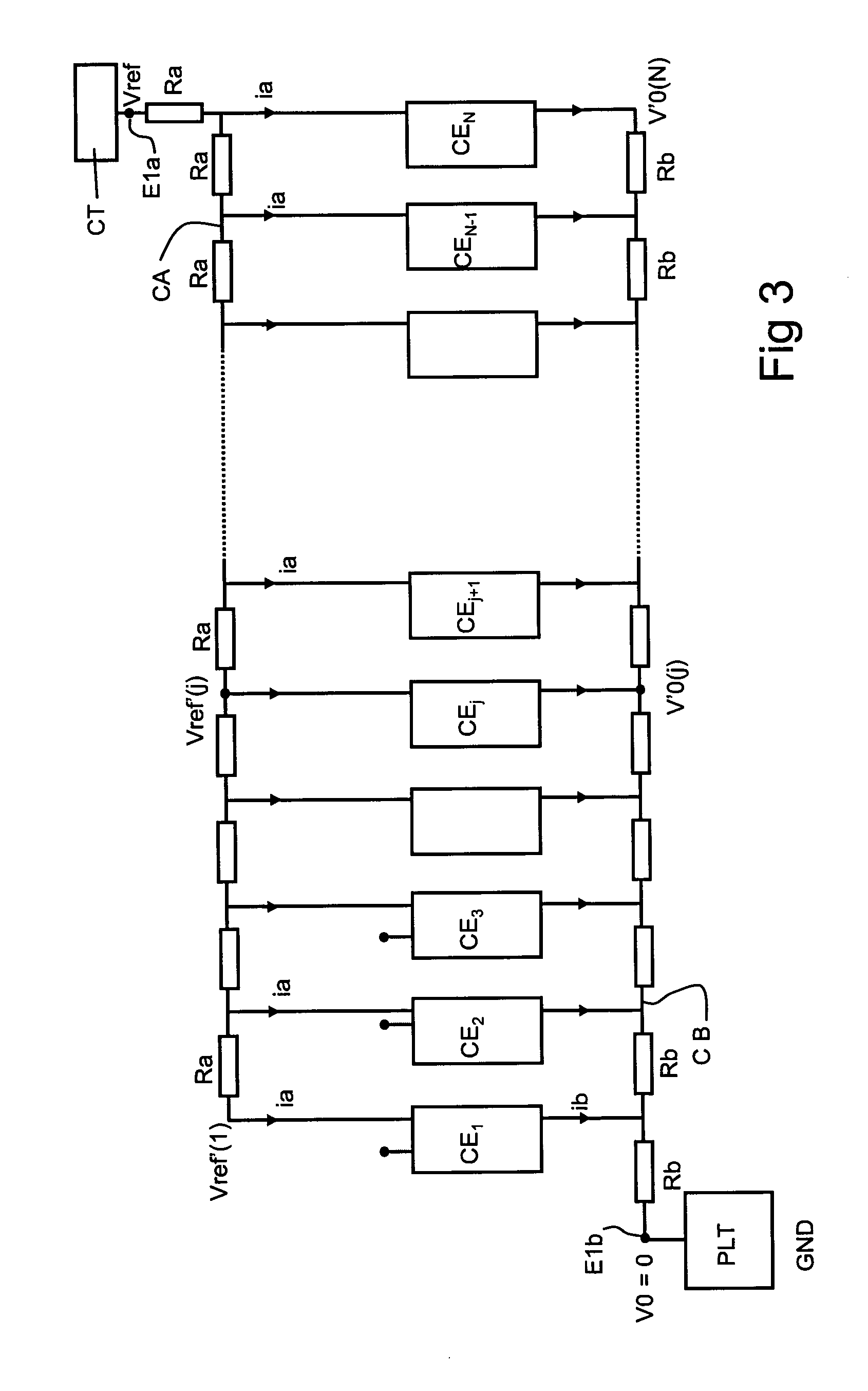
[0039]FIG. 3 represents the integrated circuit according to the invention, or more precisely the portion of integrated circuit to which the invention relates, the integrated circuit clearly being able to comprise many other elements.

[0040]The invention will be described in the context set out above, namely a precision analog-digital or digital-analog converter capable of delivering a digital value coded on 12 or 14 bits for each value of analog voltage applied to the input of the converter. The converter uses many series of current sources which are all identical; each source may consist of a transistor having its emitter (or its source) connected to a conductor which is connected to a ground potential V0, with or without emitter resistance, and its base (or its gate) connected to a conductor connected to a reference potential Vref. The invention can be applied to other integrated circuits in which the problem arises of applying a potential difference Vref−V0 to a series of many ele...


PUM


Abstract

The invention relates to an integrated circuit comprising a succession of N identical elementary circuits, juxtaposed in the order of their rank j varying from 1 to N, N being at least equal to 50, and all having to receive two reference potentials Vref and V0 supplied by two conductors. The upstream input of the second conductor is situated geographically on the side of the rank 1 of the succession of juxtaposed circuits, and the upstream input of the first conductor is situated geographically on the side of the rank N of the succession of juxtaposed circuits. This reduces the error in the potential difference applied to the elementary circuits all along the succession, an error that originates from the non-zero resistance of the conductors.
Application to analog-digital converters or digital-analog converters with high resolution (10 bits or more).

Description

RELATED APPLICATIONS[0001]The present application is based on International Application Number PCT / EP2009 / 050945 filed Jan. 28, 2009, and claims priority from French Application Number 0800678, filed Feb. 8, 2008, the disclosures of which are hereby incorporated by reference herein in their entirety.FIELD OF THE INVENTION[0002]The invention relates to integrated circuits comprising a large number of identical elementary circuits which must receive in parallel identical reference voltages from one elementary circuit to the other.BACKGROUND OF THE INVENTION[0003]A typical envisaged application is that of analog-digital converters with high resolution, typically converters of 12 or 14 bits the structure of which is highly parallel in order to make it possible to perform a very rapid conversion. The converters of the flash type, for example, have a highly parallel structure in the sense that very many individual voltage comparators simultaneously carry out a comparison operation between...

Claims


Application Information

Patent Timeline
Patent Type & Authority Applications(United States)
IPC IPC(8): H01L25/00
CPCH03K19/00369
Inventor NICOLAS, JEAN-ALAINMORRISON, RICHARD
Owner E2V SEMICON
Why Eureka
Try Eureka