Semiconductor chip package structure for achieving flip-chip type electrical connection without using wire-bonding process and method for making the same

Active Publication Date: 2011-01-27
HARVATEK CORPORATION
View PDF1 Cites 6 Cited by
  • Summary
  • Abstract
  • Description
  • Claims
  • Application Information

AI Technical Summary

Benefits of technology

[0007]In view of the aforementioned issues, the present invention provides a semiconductor chip package structure for achieving flip-chip type electrical connection without using wire-bonding process and a method for making the same. Because the semiconductor chip package structure of the present invention can achieve electrical connection without using a wire-bonding process, the present invention can omit the wire-bonding process and avoid bad electrical connection in the semiconductor chip package structure.
[0010]Therefore, the semiconductor chip package structure of the present invention can achieve electrical connection without using a wire-bonding process, so that the present invention can omit the wire-bonding process and avoid bad electrical connection in the semiconductor chip package structure.

Problems solved by technology

However, the method of the prior art not only increases manufacture time and cost, but also leads to uncertainty about the occurrence of bad electrical connections in the LED package structure of the prior art resulting from the wire-bonding process.

Method used


Image

  • Semiconductor chip package structure for achieving flip-chip type electrical connection without using wire-bonding process and method for making the same
  • Semiconductor chip package structure for achieving flip-chip type electrical connection without using wire-bonding process and method for making the same
  • Semiconductor chip package structure for achieving flip-chip type electrical connection without using wire-bonding process and method for making the same

Examples


Embodiment Construction

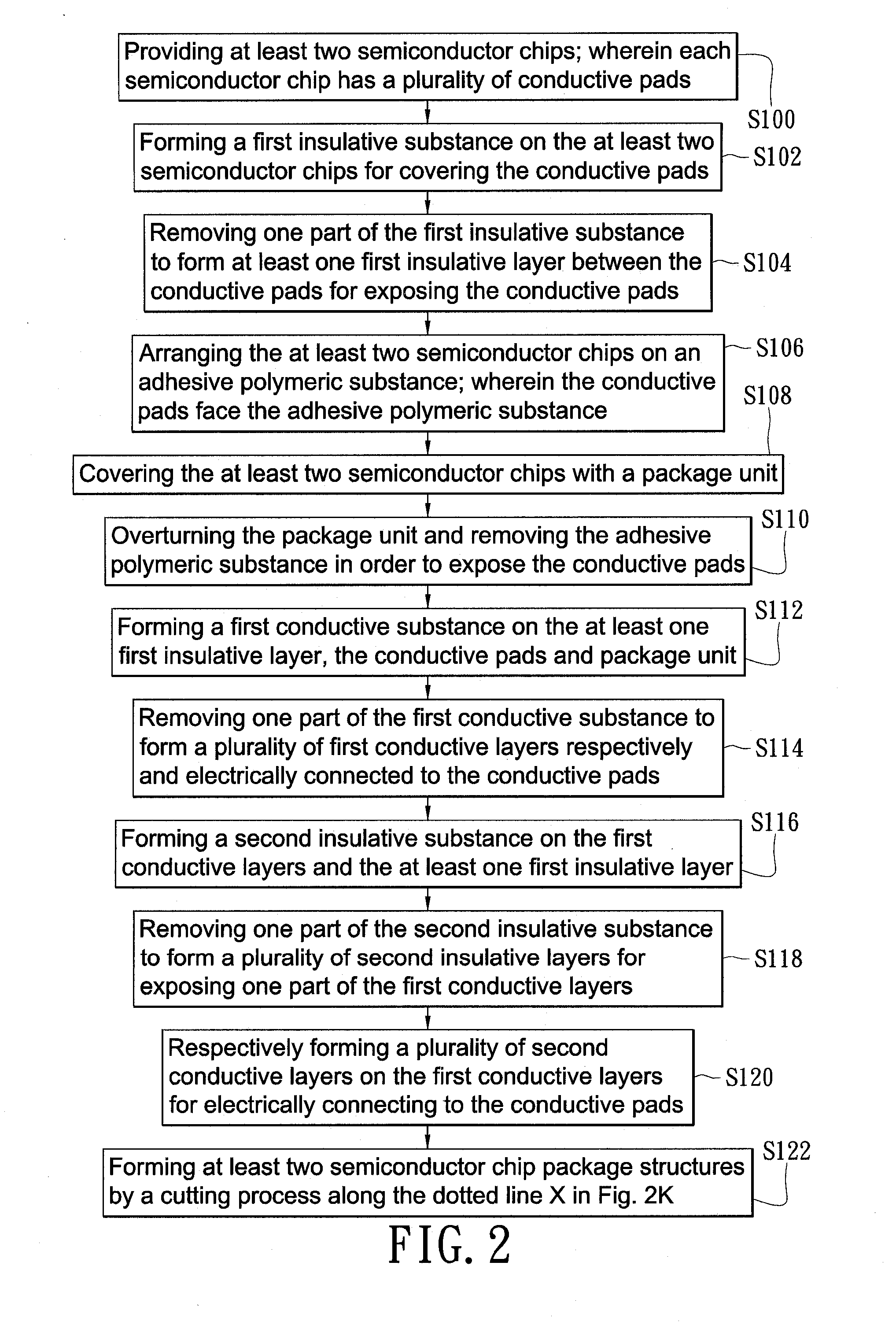
[0015]Referring to FIGS. 2 and 2A-2L, the present invention provides a method of making semiconductor chip package structures for achieving flip-chip type electrical connection without using wire-bonding process, including as follows:

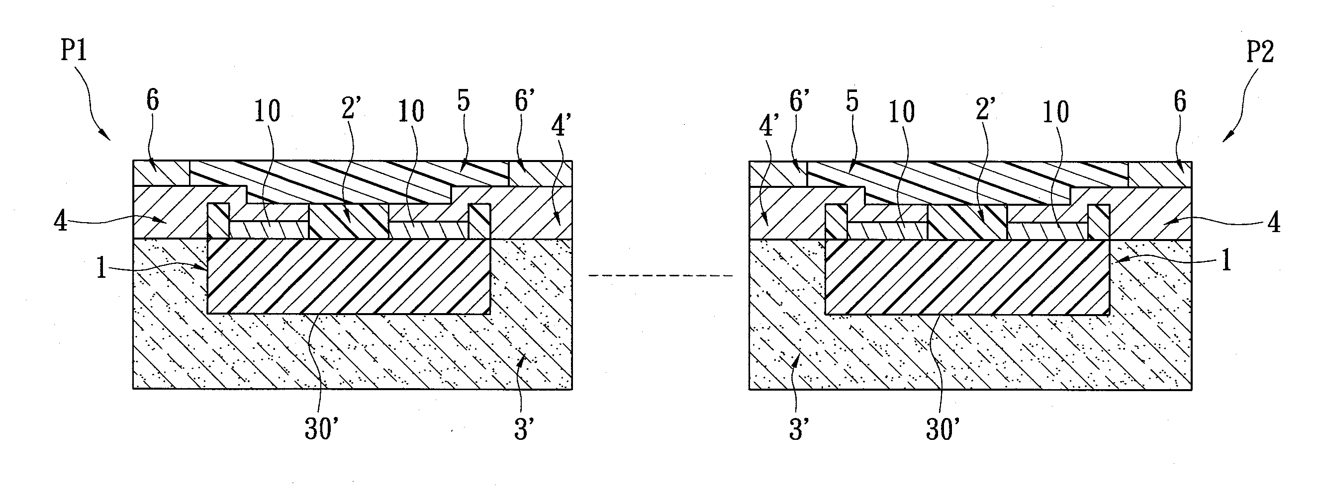
[0016]Step S100 is: referring to FIGS. 2 and 2A, providing at least two semiconductor chips 1; wherein each semiconductor chip 1 has a plurality of conductive pads 10.

[0017]Step S102 is: referring to FIGS. 2 and 2B, forming a first insulative substance B1 on the at least two semiconductor chips 1 for covering the conductive pads 10. In addition, the first insulative substance B1 is formed on the at least two semiconductor chips 1 by printing, coasting or spraying, and the first insulative substance B1 is hardened by pre-curing.

[0018]Step S104 is: referring to FIGS. 2 and 2C, removing one part of the first insulative substance B1 to form at least one first insulative layer 2 between the conductive pads 10 for exposing the conductive pads 10. In other wor...


PUM


Abstract

A semiconductor chip package structure for achieving flip-chip electrical connection without using a wire-bonding process includes a package unit, a semiconductor chip, a first insulative layer, first conductive layers, a second insulative layer, and second conductive layers. The package unit has a receiving groove. The semiconductor chip is received in the receiving groove and has a plurality of conductive pads disposed on its top surface. The first insulative layer is formed between the conductive pads to insulate the conductive pads. The first conductive layers are formed on the first insulative layer and the package unit, and one side of each first conductive layer is electrically connected to the corresponding conductive pad. The second insulative layer is formed between the first conductive layers in order to insulate the first conductive layers from each other. The second conductive layers are respectively formed on the other opposite sides of the first conductive layers.

Description

BACKGROUND OF THE INVENTION[0001]1. Field of the Invention[0002]The present invention relates to a semiconductor chip package structure and a method for making the same, in particular, to a semiconductor chip package structure for achieving flip-chip type electrical connection without using wire-bonding process and a method for making the same.[0003]2. Description of the Related Art[0004]Referring to FIG. 1, a known LED package structure is packaged via a wire-bonding process. The known LED package structure includes a substrate 1a, an LED (light emitting diode) 2a disposed on the substrate, two wires 3a, and a phosphor resin body 4a. [0005]The LED 2a has a light-emitting surface 20a opposite to the substrate 1a. The LED 2a has a positive pole area 21a and a negative pole area 22a electrically connected to two corresponding positive and negative pole areas 11a, 12a of the substrate 1a via the two wires 3a respectively. Moreover, the LED 2a and the two wires 3a are covered with the p...

Claims


Application Information

Patent Timeline
IPC IPC(8): H01L33/00H01L31/18H01L21/78H01L31/02H01L23/48
CPCH01L21/561H01L21/565H01L2924/12041H01L2224/04042H01L2924/00014H01L2924/01006H01L2924/01005H01L24/48H01L2924/09701H01L21/568H01L23/3121H01L24/03H01L24/05H01L24/96H01L33/62H01L2224/05599H01L2224/48091H01L2224/48247H01L2924/01027H01L2924/01078H01L2924/00H01L2924/181H01L2924/14H01L2224/24137H01L2924/00012H01L2224/45099H01L2224/45015H01L2924/207
Inventor WANG, BILYYANG, HUNG-CHOUCHANG, JENG-RU
Owner HARVATEK CORPORATION
Why Eureka
Try Eureka