Methods for fabricating non-planar electronic devices having sidewall spacers formed adjacent selected surfaces

a technology of sidewall spacers and electronic devices, which is applied in the direction of decorative surface effects, electrical equipment, decorative arts, etc., can solve the problems of affecting the fabrication efficiency of finfets and other non-planar multi-gate devices, and affecting the quality of electronic devices

Inactive Publication Date: 2011-01-27
GLOBALFOUNDRIES INC
View PDF2 Cites 57 Cited by
  • Summary
  • Abstract
  • Description
  • Claims
  • Application Information

AI Technical Summary

Benefits of technology

[0006]Methods are provided for fabricating an electronic device having at least one sidewall spacer formed adjacent a selected surface. In one embodiment, the method includes the step of depositing spacer material adjacent first and second raised structures formed on the substrate and extending along substantially perpendicular axes. The method further includes the step of selectively removing spacer material laterally adjacent one of the first raised structure and

Problems solved by technology

While providing the advantages noted above, FinFETs and other non-planar multi-gate devices (e.g., triFETs) can be somewhat difficult to fabricate due to their unique topographies.
For example, in the case of a simplified FinFET including two fins and one gate, it is difficult to form sidewall spacers adjacent opposing sidewalls of the gate without simultaneously forming parasitic sidewall spacers adjacent opposing sidewalls of the fins.
While permitting the selective formation of sidewall spacers adjacent a gate, the above-described fabrication technique is limited in several respects.
Due to its severity, this over-etch has several undesirable consequences.
First, a considerable volume of spacer material is removed from the gate during the etching process thus potentially exposing the fin-gate

Method used


Image

  • Methods for fabricating non-planar electronic devices having sidewall spacers formed adjacent selected surfaces
  • Methods for fabricating non-planar electronic devices having sidewall spacers formed adjacent selected surfaces
  • Methods for fabricating non-planar electronic devices having sidewall spacers formed adjacent selected surfaces

Examples


Embodiment Construction

[0011]The following Detailed Description is merely exemplary in nature and is not intended to limit the invention or the application and uses of the invention. Furthermore, there is no intention to be bound by any expressed or implied theory presented in the preceding Technical Field, Background, Brief Summary, or the following Detailed Description.

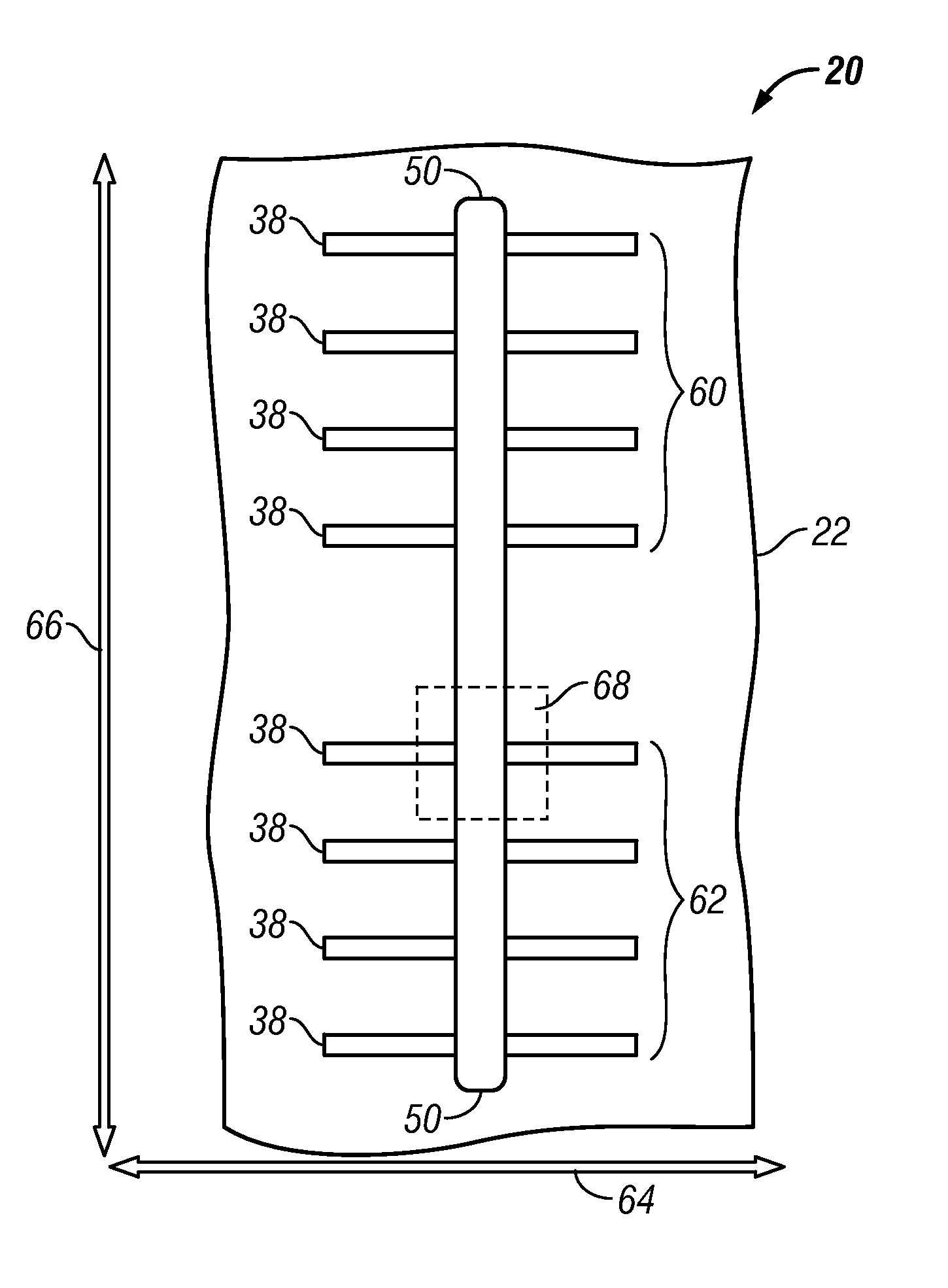
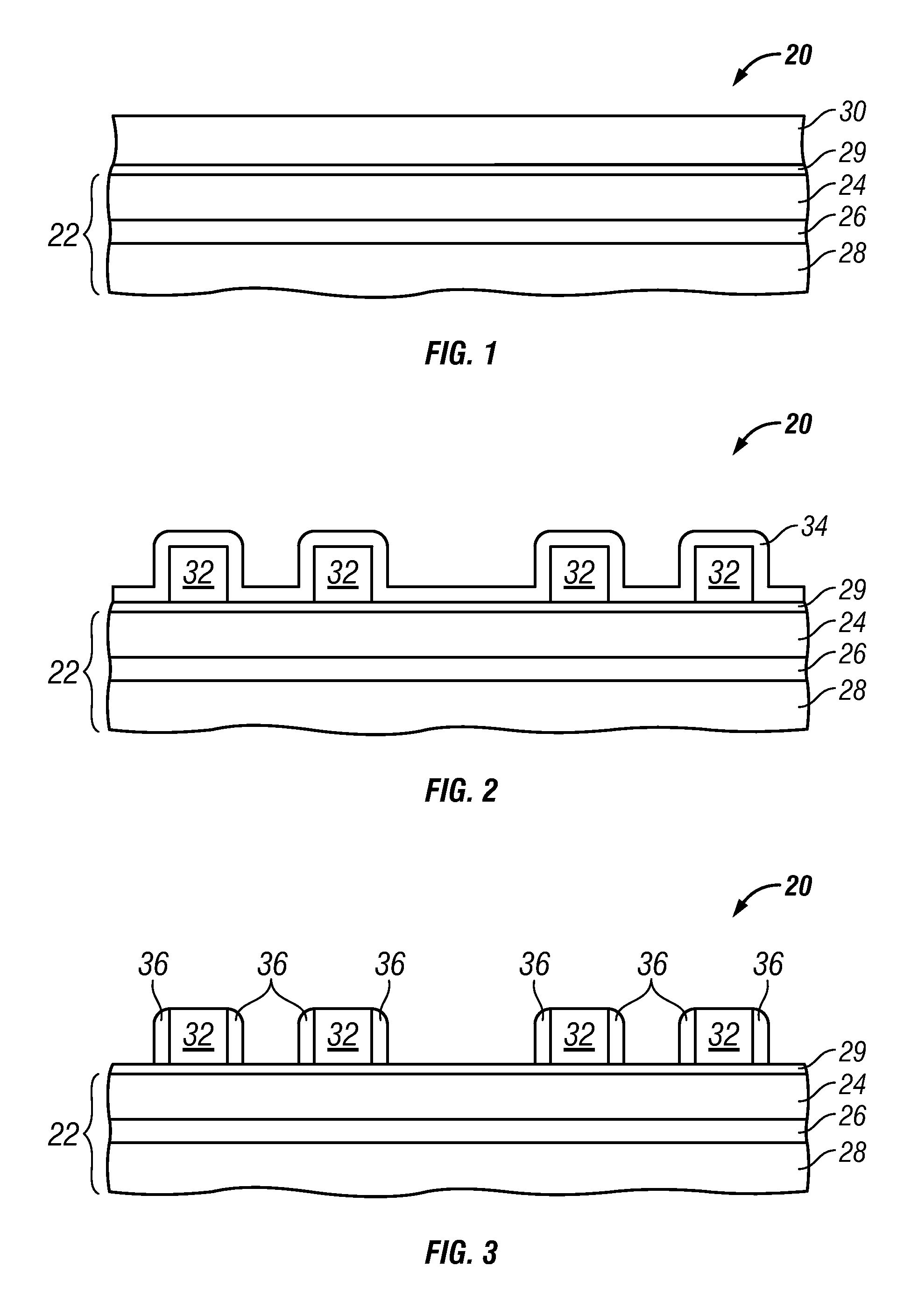
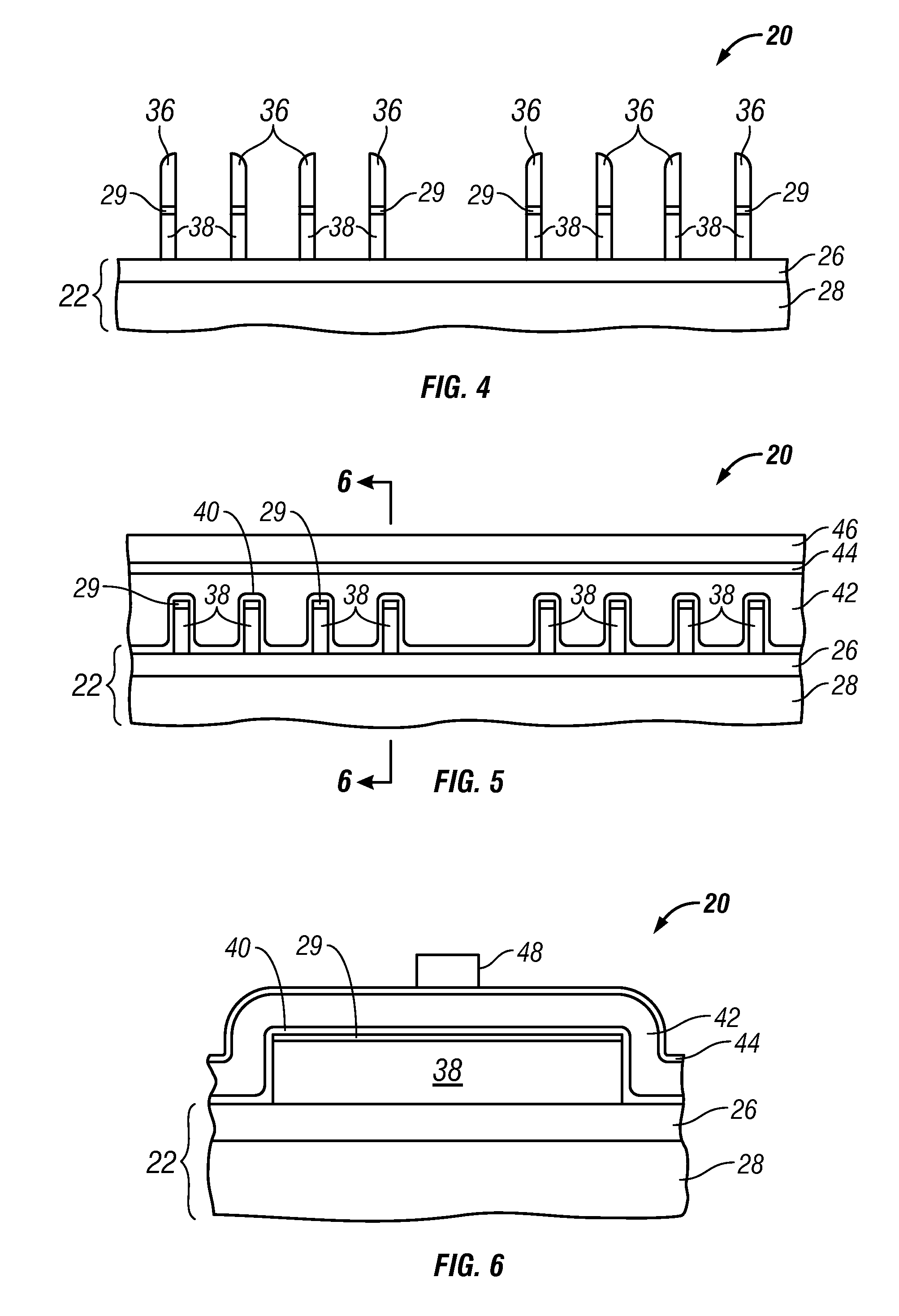
[0012]The following describes multiple exemplary embodiments of a fabrication method wherein sidewall spacers are selectively formed adjacent opposing sidewalls of one or more raised structures on a small scale electronic device. Relative to conventional spacer-forming techniques typically utilized in the fabrication of non-planar, multi-gate semiconductor devices, embodiments of the method described herein significantly reduce or eliminate over-etching requirements. Embodiments of the method described herein are especially well-suited for selectively producing sidewall spacers adjacent opposing sidewalls of one or more gate stacks includ...


PUM

PropertyMeasurementUnit
Angleaaaaaaaaaa
Angleaaaaaaaaaa
Angleaaaaaaaaaa

Abstract

Methods are provided for fabricating an electronic device having at least one sidewall spacer formed adjacent a selected surface. In one embodiment, the method includes the step of depositing spacer material adjacent first and second raised structures formed on the substrate and extending along substantially perpendicular axes. The method further includes the step of selectively removing spacer material laterally adjacent one of the first raised structure and the second raised structure. During the step of selectively removing, the electronic device is bombarded with ions from a first predetermined direction forming a first predetermined grazing angle with the substrate such that the spacer material adjacent a first sidewall of the first raised structure is substantially exposed to the ion bombardment while the spacer material adjacent opposing sidewalls of the second raised structure is substantially shielded therefrom.

Description

TECHNICAL FIELD[0001]The present invention relates generally to the fabrication of small scale electronic devices and, more particularly, to methods for fabricating non-planar semiconductor devices (e.g., FinFETs) and other small scale electronic devices wherein sidewall spacers are formed adjacent a first raised structure (e.g., a fin structure) without simultaneously forming sidewall spacers adjacent a second raised structure (e.g., a gate stack).BACKGROUND[0002]In contrast to conventional planar metal-oxide-semiconductor field-effect transistors (“MOSFETs”), multi-gate transistors incorporate two or more gates into a single device. Relative to single gate transistors, multi-gate transistors reduce off-state current leakage, increase on-state current flow, and reduce overall power consumption. Multi-gate devices having non-planar topographies also tend to be more compact than conventional planar transistors and consequently permit higher device densities to be achieved. One known ...

Claims


Application Information

Patent Timeline
IPC IPC(8): H01L21/3065
CPCH01L21/3086H01L21/31116H01L29/785H01L21/845H01L29/66795H01L21/32139
Inventor JOHNSON, FRANK SCOTT
Owner GLOBALFOUNDRIES INC
Why Eureka
Try Eureka