Methods of changing threshold voltages of semiconductor transistors by ion implantation

Inactive Publication Date: 2009-05-14
GLOBALFOUNDRIES INC
View PDF2 Cites 29 Cited by
  • Summary
  • Abstract
  • Description
  • Claims
  • Application Information

AI Technical Summary

Problems solved by technology

Unfortunately, this spacing is such that the blocking resist used to allow such threshold-adjusting implants into one FET and not an adjacent one, prohibits the use of tilted, or angled, implants that are needed to dope the fins in a uniform manner.

Method used


Image

  • Methods of changing threshold voltages of semiconductor transistors by ion implantation
  • Methods of changing threshold voltages of semiconductor transistors by ion implantation
  • Methods of changing threshold voltages of semiconductor transistors by ion implantation

Examples


Embodiment Construction

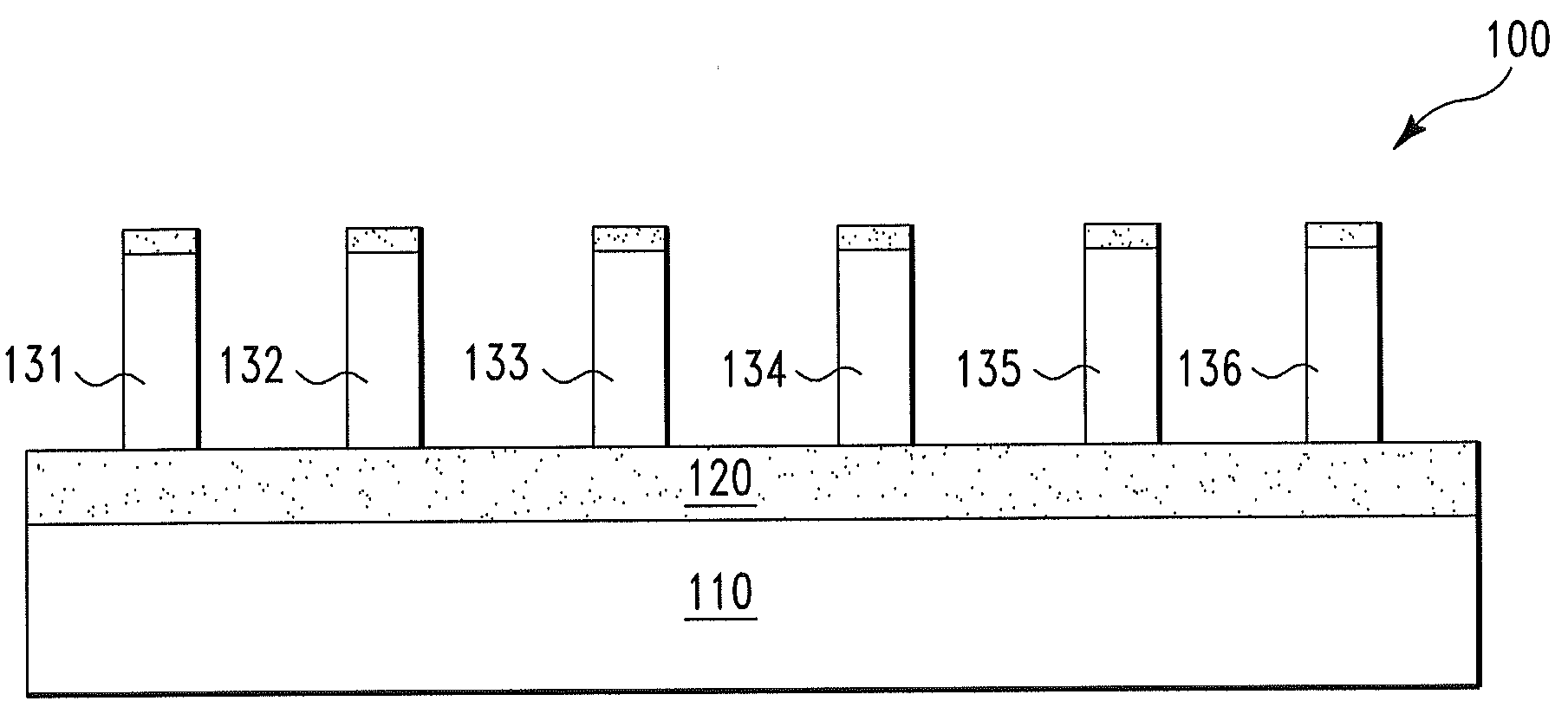
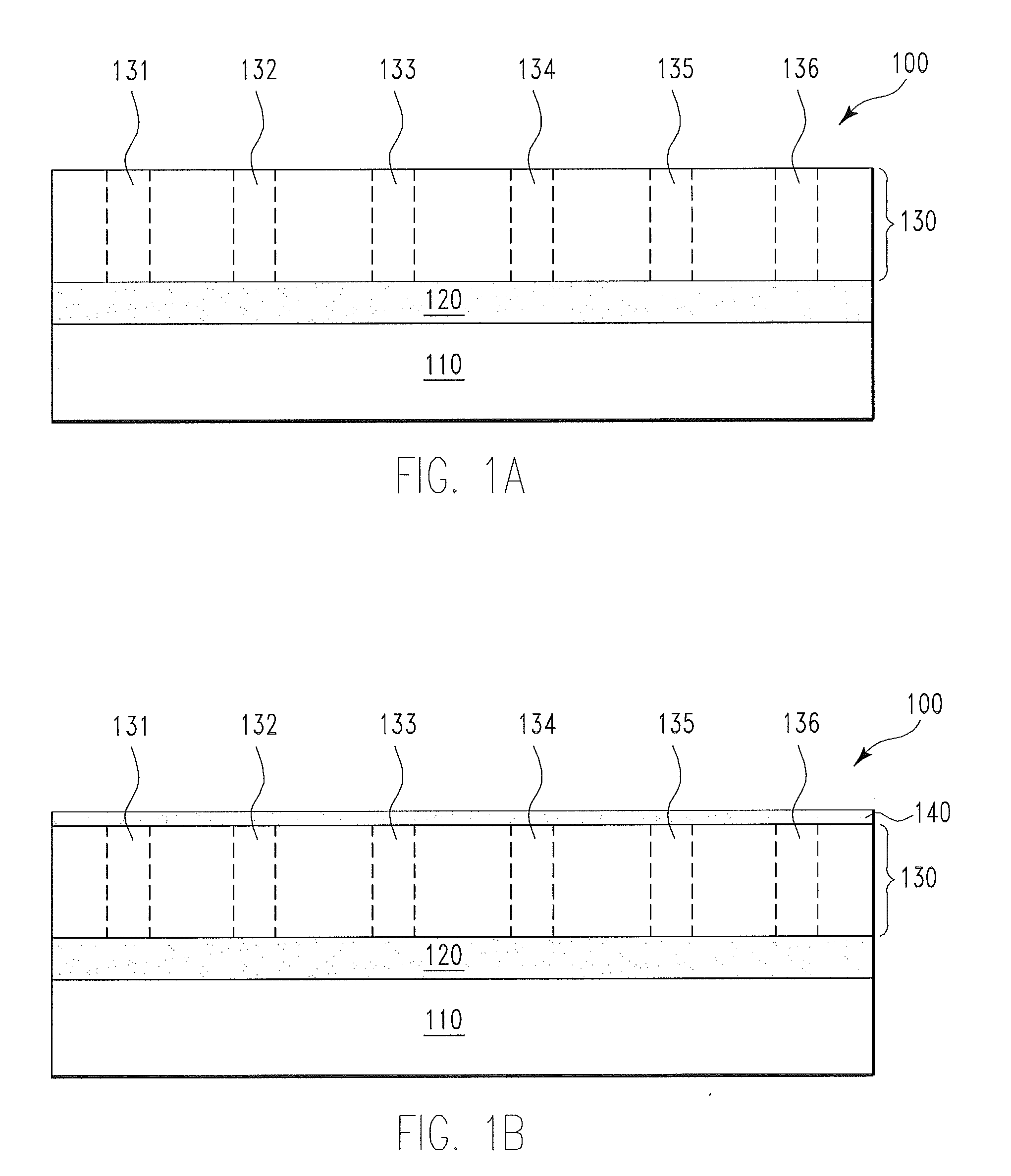
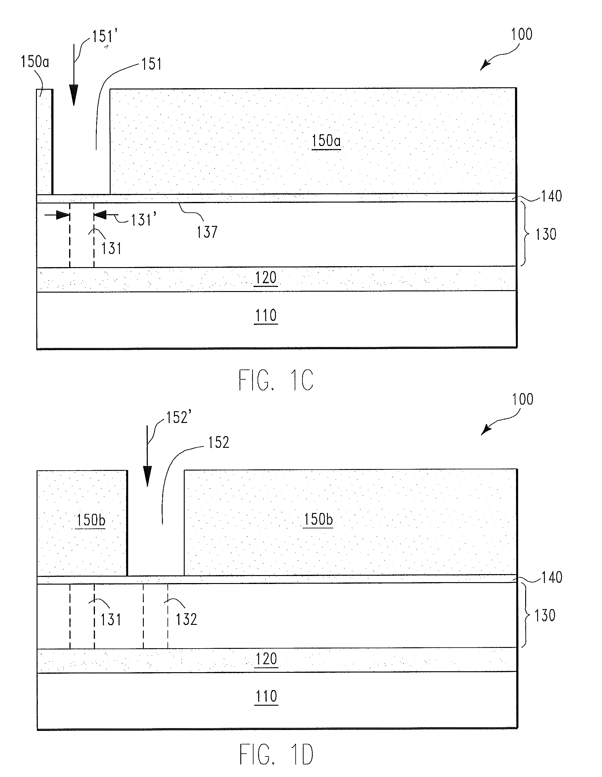
[0006]FIGS. 1A-1M show cross-section views used to illustrate a fabrication process of a semiconductor structure 100, in accordance with embodiments of the present invention. More specifically, with reference to FIG. 1A, the fabrication process of the semiconductor structure 100 starts with an SOI (Silicon On Insulator) substrate 110+120+130. The SOI substrate 110+120+130 comprises a silicon substrate 110, a BOX (buried oxide) layer 120 on top of the silicon substrate 110, and an active silicon layer 130 on top of the BOX layer 120. The SOI substrate 110+120+130 can be formed by a conventional method. Alternatively, the substrate can comprise a conventional (bulk) silicon wafer, and furthermore, may further comprise an isolation layer comprising either doped silicon or silicon-germanium in lieu of the BOX layer 120.

[0007]Consider the case where FETs (field effect transistors) are to be formed on the semiconductor structure 100 of FIG. 1A. More specifically, consider the case where a...


PUM


Abstract

A method for forming a semiconductor structure. The method includes providing a semiconductor structure including a semiconductor substrate. The semiconductor substrate includes (i) a top substrate surface which defines a reference direction perpendicular to the top substrate surface and (ii) a semiconductor body region. The method further includes implanting an adjustment dose of dopants of a first doping polarity into the semiconductor body region by an adjustment implantation process. Ion bombardment of the adjustment implantation process is in the reference direction. The method further includes (i) patterning the semiconductor substrate resulting in side walls of the semiconductor body region being exposed to a surrounding ambient and then (ii) implanting a base dose of dopants of a second doping polarity into the semiconductor body region by a base implantation process. Ion bombardment of the base implantation process is in a direction which makes a non-zero angle with the reference direction.

Description

FIELD OF THE INVENTION[0001]The present invention relates generally to methods for changing threshold voltages of transistors and more particularly to methods for changing threshold voltages of transistors by ion implantation.BACKGROUND OF THE INVENTION[0002]In a conventional process for changing threshold voltage of a transistor on a chip, the semiconductor body of the transistor can be doped with dopants by ion implantation. Control of the value of the threshold voltage is critical to good performance and low power consumption of the circuits employing the transistors. In Multi-Gate FETs (MuGFETs), such as FinFETs, Tri-Gate, and other related structures, doping the MuGFET body is best performed with angled implants at some point following fin (body) formation, as this allows total dose delivery to the body to be minimally affected by incidental variations in fin dimensions. When multiple threshold-voltages are required for the same polarity (e.g. n-type) FET, it is desirable that ...

Claims


Application Information

Patent Timeline
Patent Type & Authority Applications(United States)
IPC IPC(8): H01L21/265
CPCH01L21/26586H01L21/823431H01L29/66803H01L29/66795H01L29/105
Inventor CLARK, JR., WILLIAM F.NOWAK, EDWARD JOSEPH
Owner GLOBALFOUNDRIES INC
Why Eureka
Try Eureka