Stress tunable tantalum and tantalum nitride films

a technology of tantalum and nitride, applied in the field of tantalum and tantalum nitride films, can solve problems such as feature distortion or even deformation on the substrate (typically a silicon wafer) surfa

Inactive Publication Date: 2002-12-03
APPLIED MATERIALS INC
View PDF19 Cites 31 Cited by
  • Summary
  • Abstract
  • Description
  • Claims
  • Application Information

AI Technical Summary

Problems solved by technology

In the alternative, the film stress can cause feature distortion on the substrate (typically a silicon wafer) surface or even deformation of a thin wafer.

Method used


Image

  • Stress tunable tantalum and tantalum nitride films
  • Stress tunable tantalum and tantalum nitride films
  • Stress tunable tantalum and tantalum nitride films

Examples


example two

When IMP-sputtered tantalum film was produced, a high density, inductively coupled RF plasma was generated in the region between the target cathode and the substrate by applying RF power to a coil (having from 1 to 3 turns) over a range from about 400 kHz to about 13.56 MHZ (preferably about 2 MHZ). Two hundred (200) mm sample surfaces were IMP sputter-deposited at a sample surface temperature of about 25.degree. C., in argon, at pressures ranging from about 10 mT to about 60 mT. The distance from the cathode to the sample was typically about 14 cm. The DC power to the tantalum target was adjusted over a range from about 1 kW to about 8 kW (preferably, about 1 kW to about 3 kW). The wattage to the RF power coil was adjusted over a range from about 1.0 kW to about 5 kW (preferably, about 1.0 kW to about 3 kW). An AC bias power ranging from about 0 W to about 500 W was used.

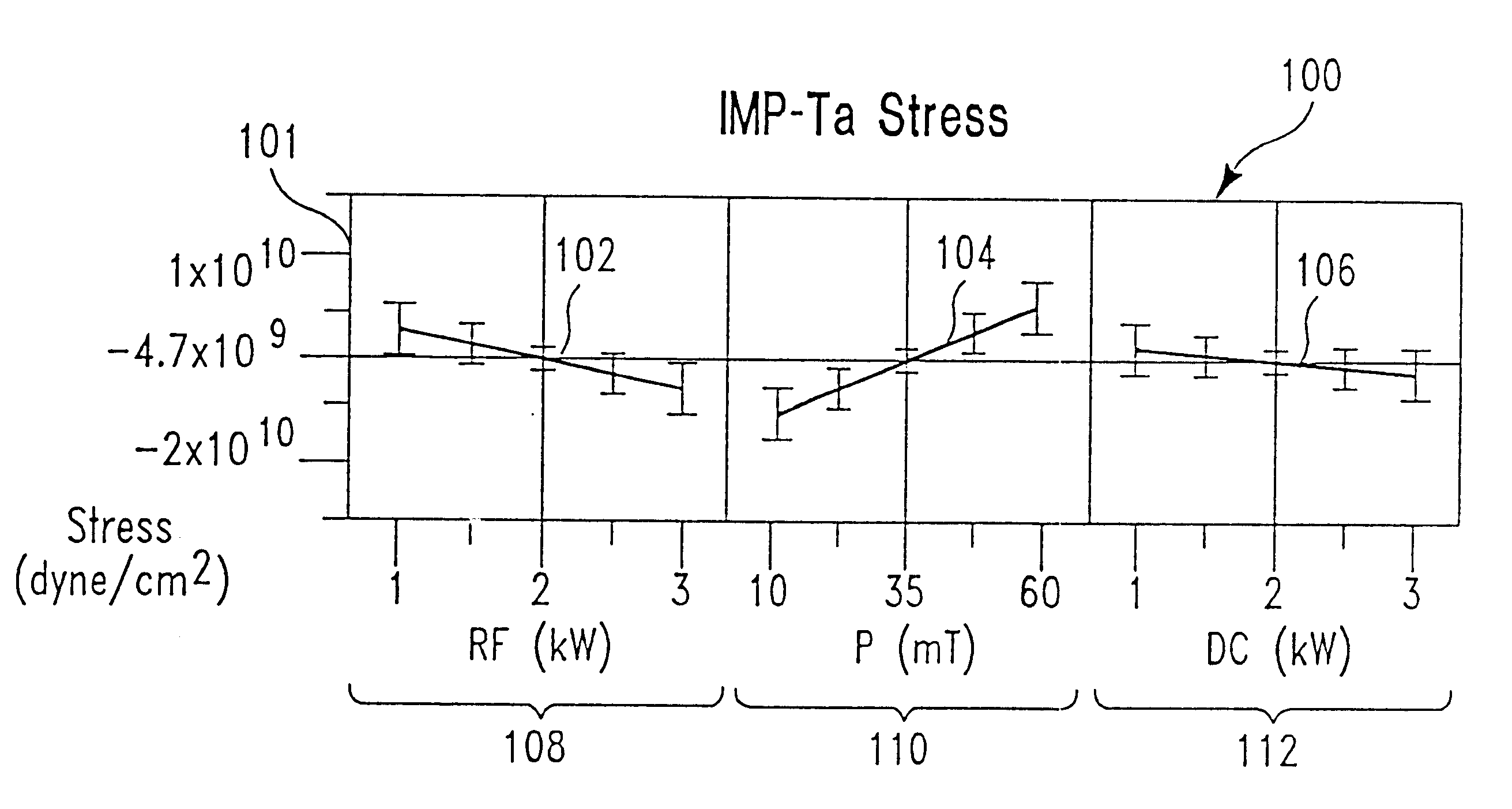
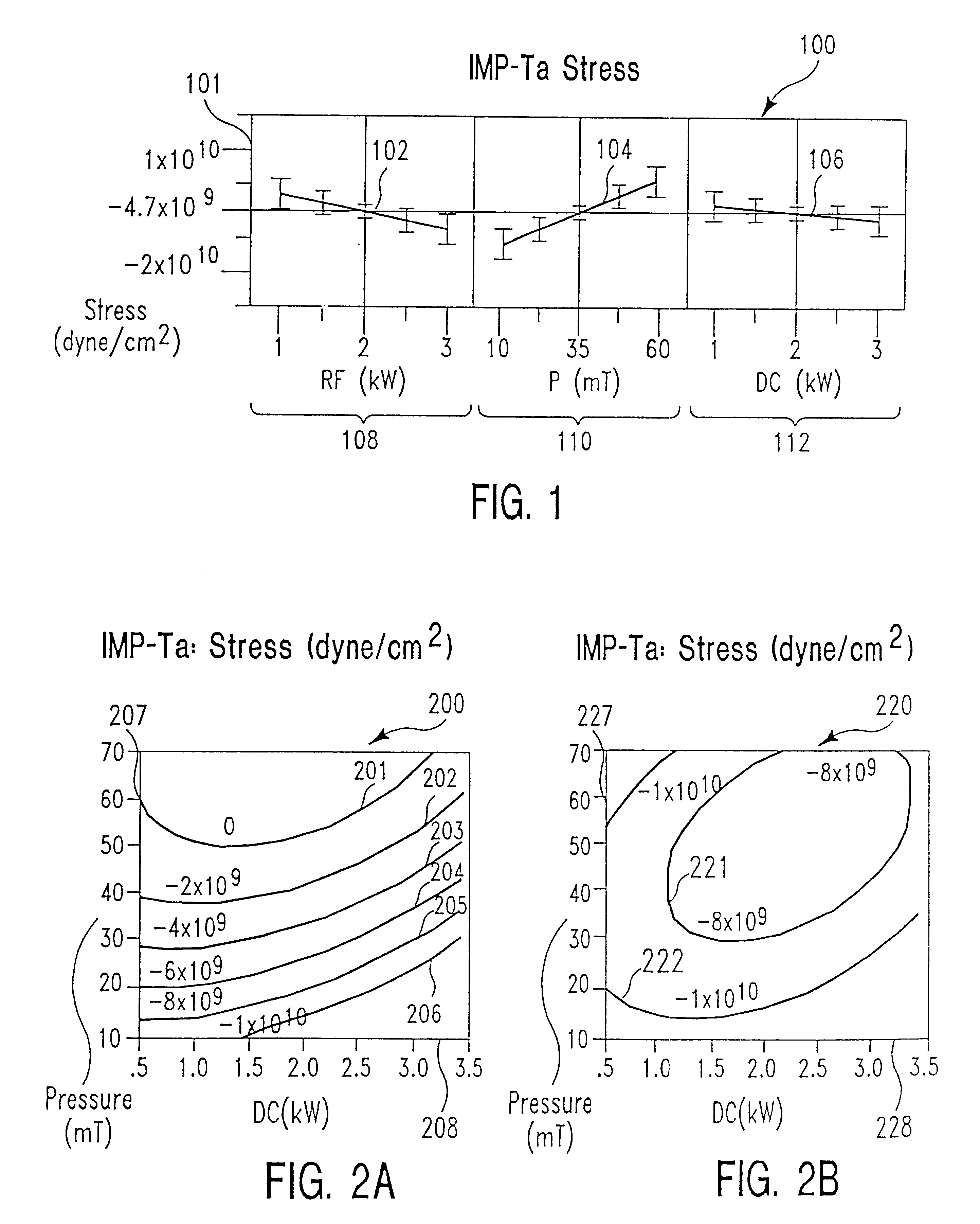
FIG. 1 shows a graph 100 of the residual film stress 101 of the tantalum film in dynes / cm.sup.2, as a function o...

example three

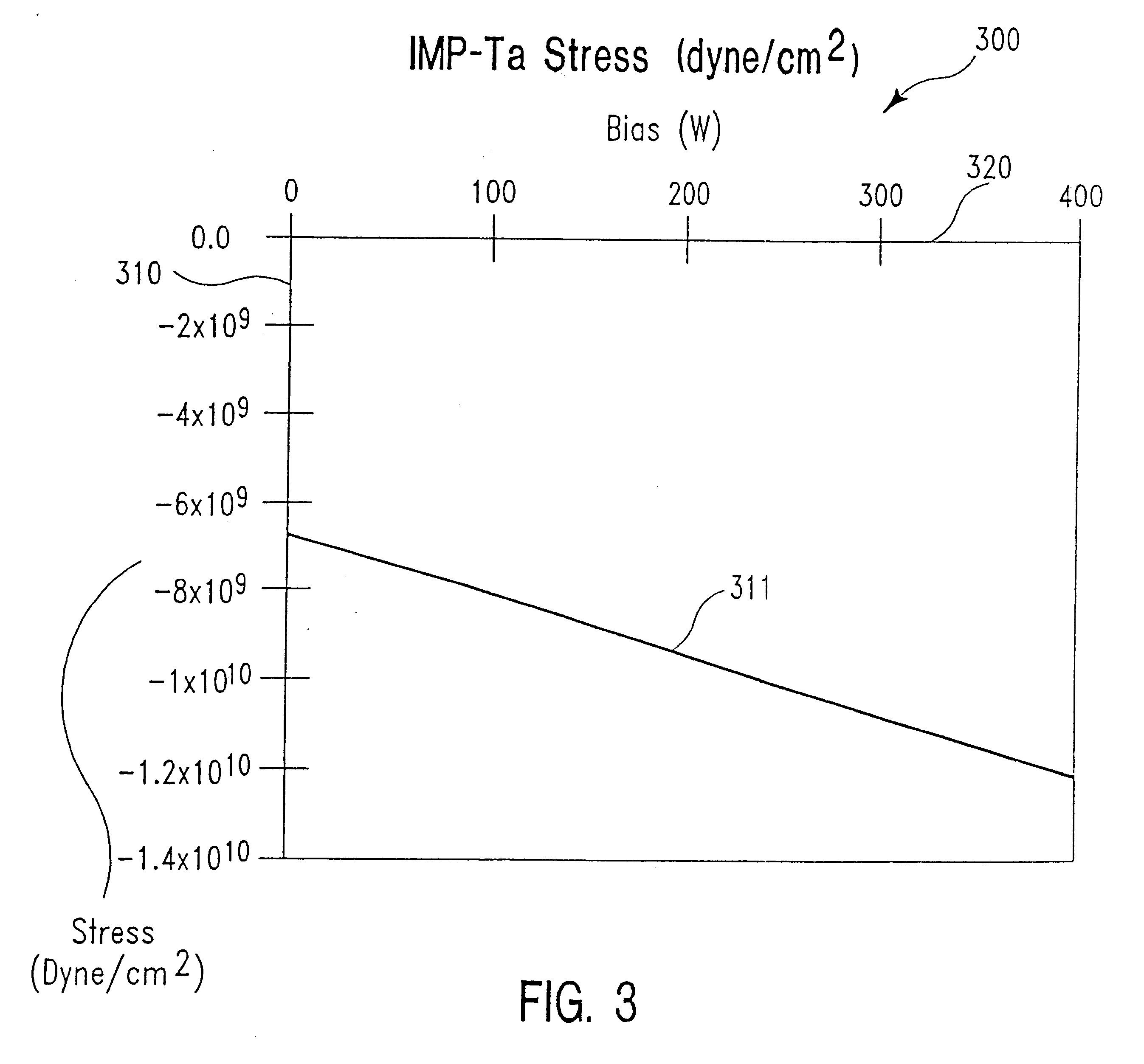
The effect of the increase in ion bombardment of a depositing film surface, which can be achieved by increasing the DC offset bias voltage of the substrate onto which the film is deposited, is illustrated in FIG. 3. Graph 300 shows the residual stress 311 in dynes / cm.sup.2 310 as a function of the AC bias power 320 in Watts. The corresponding substrate DC offset bias voltage ranges from about 0 V to about -150 V.

example four

When tantalum nitride films are produced, the structure of the tantalum nitride depends on the amount of nitrogen in the tantalum nitride compound (film). FIGS. 4 and 5 show the chemical composition and resistivity of tantalum nitride films produced using gamma sputtering and IMP sputtering techniques, respectively. The chemical composition (atomic nitrogen content) of the film is shown as a function of the nitrogen gas flow rate to the process chamber in which the TaN.sub.x film is produced.

FIG. 4, graph 400, shows the nitrogen content 410 of the gamma-sputtered tantalum nitride film in atomic % 413, as a function of the nitrogen flow rate 416 in sccm to the process vessel. A two hundred (200) mm diameter sample surface was gamma sputter-deposited at a sample surface temperature of about 25.degree. C., in an argon / nitrogen atmosphere, at a pressure of about 1.5 mT, where the argon gas feed was about 15 sccm, and the nitrogen flow rate 416 was as shown on graph 400. The "throw" dist...


PUM

PropertyMeasurementUnit
temperatureaaaaaaaaaa

Abstract

The present disclosure pertains to our discovery that residual stress residing in a tantalum film or tantalum nitride film can be controlled (tuned) during deposition by adjusting at least two particular process variables which have counteracting effects on the residual film stress. By tuning individual film stresses within a film stack, it is possible to balance stresses within the stack. Process variables of particular interest include: power to the sputtering target process chamber pressure (i.e., the concentration of various gases and ions present in the chamber); substrate DC offset bias voltage (typically an increase in the AC applied substrate bias power); power to an ionization source (typically a coil); and temperature of the substrate upon which the film is deposited. The process chamber pressure and the substrate offset bias most significantly affect the film tensile and compressive stress components, respectively. The most advantageous tuning of a sputtered film is achieved using high density plasma sputter deposition, which provides for particular control over the ion bombardment of the depositing film surface. When the tantalum or tantalum nitride film is deposited using high density plasma sputtering, power to the ionization source can be varied for stress tuning of the film. We have been able to reduce the residual stress in tantalum or tantalum nitride films deposited using high density plasma sputtering to between about 6x10+9 dynes / cm2 and about -6x10+9 dynes / cm2 using techniques described herein.

Description

1. Field of the InventionThe present invention pertains to tantalum and tantalum nitride films which can be stress-tuned to be in tension or in compression or to have a particularly low stress, and to a method of producing such films. These stress-tuned films are particularly useful in semiconductor interconnect structures, where they can be used to balance the stress within a stack of layers, which includes a combination of barrier layers, wetting layers, and conductive layers, for example. The low stress tantalum and tantalum nitride films are particularly suited for the lining of vias and trenches having high aspect ratios.2. Brief Description of the Background ArtA typical process for producing a multilevel structure having feature sizes in the range of 0.5 micron (.mu.m) or less would include: blanket deposition of a dielectric material; patterning of the dielectric material to form openings; deposition of a diffusion barrier layer and, optionally, a wetting layer to line the o...

Claims


Application Information

Patent Timeline
Patent Type & Authority Patents(United States)
IPC IPC(8): C23C14/16C23C14/06H01L21/285H01L21/02H01L23/532H01L21/70H01L23/52H01L21/768C23C14/58C23C14/00C23C14/14C23C14/34C23C14/35
CPCC23C14/0036C23C14/0641C23C14/16C23C14/345C23C14/3492C23C14/358C23C14/5833H01L21/2855H01L21/76838H01L21/76841H01L21/76843H01L21/76862H01L21/76864H01L23/53233H01L23/53238H01L2924/0002H01L2924/00C23C14/0042C23C14/165C23C14/541
Inventor CHIANG, TONYDING, PEIJUNCHIN, BARRY L.SUN, BINGXI
Owner APPLIED MATERIALS INC
Why Eureka
Try Eureka