Plasma apparatus and method capable of adaptive impedance matching

a technology of impedance matching and apparatus, applied in the direction of mechanical apparatus, chucks, manufacturing tools, etc., can solve the problems of destroying the electric properties of mos devices, causing scraped wafers, and incomplete dielectric layer deposition,

Active Publication Date: 2005-03-17
MARLIN SEMICON LTD
View PDF17 Cites 30 Cited by
  • Summary
  • Abstract
  • Description
  • Claims
  • Application Information

AI Technical Summary

Benefits of technology

[0009] The main purpose of the present invention is to solve the aforementioned problem of the non-uniform voltage potential difference between the plasma and the bi-polar electrostatic chuck. The present invention provides a solution which adds an impedance-matching circuit between the AC bias power for generating the ion-bombardment and the bi-polar electrostatic chuck. The impedance-matching circuit can regulate the impedance of the inner electrode and the outer electrode of the bi-polar electrostatic chuck to balance the inner electrode power output and the outer electrode power output. Furthermore, the impedance-matching circuit can lead to a uniform voltage potential difference between the plasma and the bi-polar electrostatic chuck to avoid the gate oxide damage caused by plasma. According to the experiment results, the fail rate of dies of a wafer decreases from 30%˜60% without adding the impedance-matching circuit to 0%˜2% with adding the impedance-matching circuit.

Problems solved by technology

The gaps of high aspect ration will let the deposition of dielectric layers become incomplete and form voids in the dielectric layers.
These voids in the dielectric layers will damage electric properties of MOS devices and lead to scraped wafers.
If the voltage potential difference between the plasma 16 and the electrostatic chuck 20 distributes extremely non-uniformly, the produced currents will damage gate oxides of MOS devices.

Method used


Image

  • Plasma apparatus and method capable of adaptive impedance matching
  • Plasma apparatus and method capable of adaptive impedance matching
  • Plasma apparatus and method capable of adaptive impedance matching

Examples


Embodiment Construction

[0021] Some embodiments of the invention will be described exquisitely as below. Besides, the invention can also be practiced extensively in other embodiments. That is to say, the scope of the invention should not be restricted by the proposed embodiments. The scope of the invention should be based on the claims proposed later.

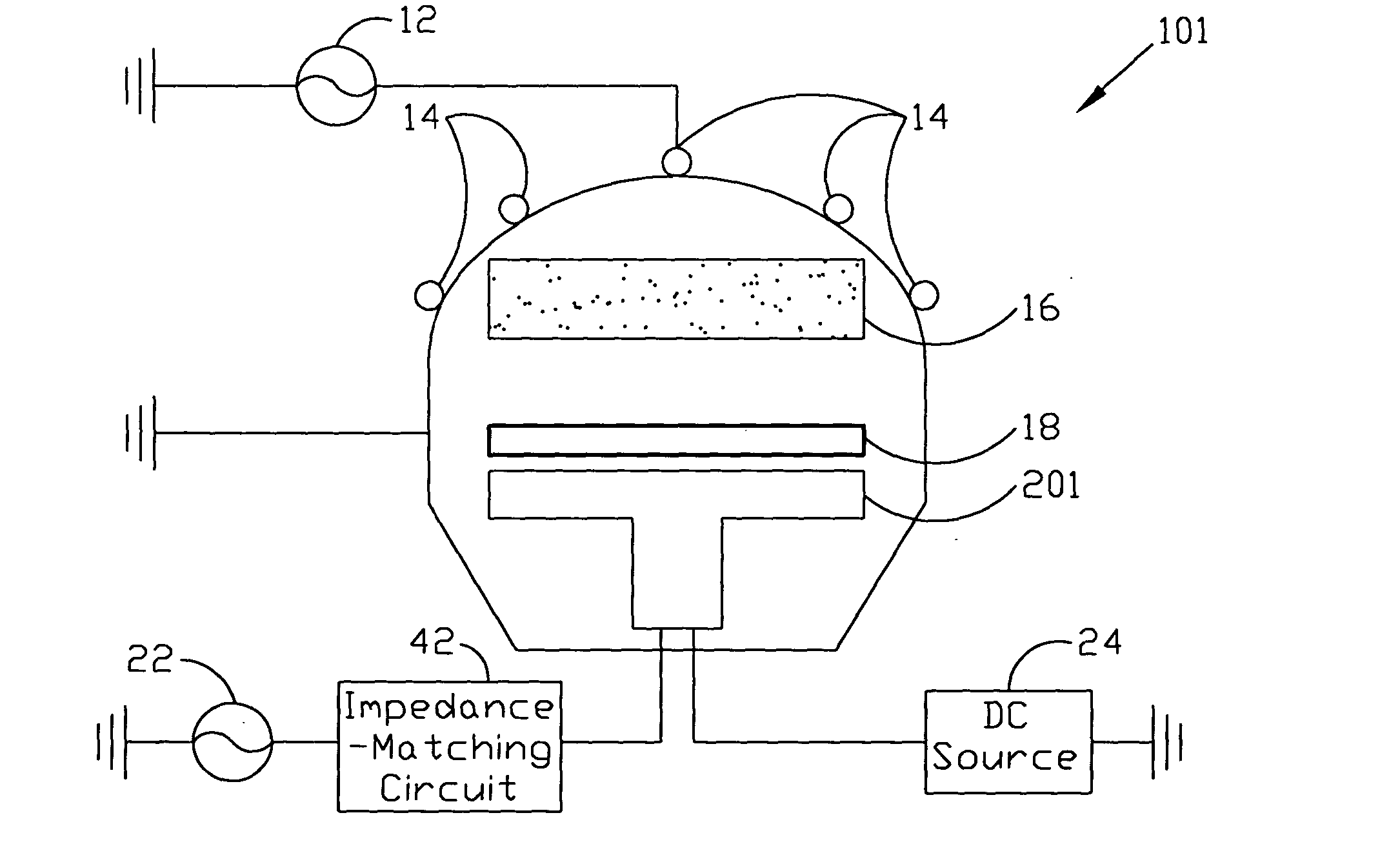
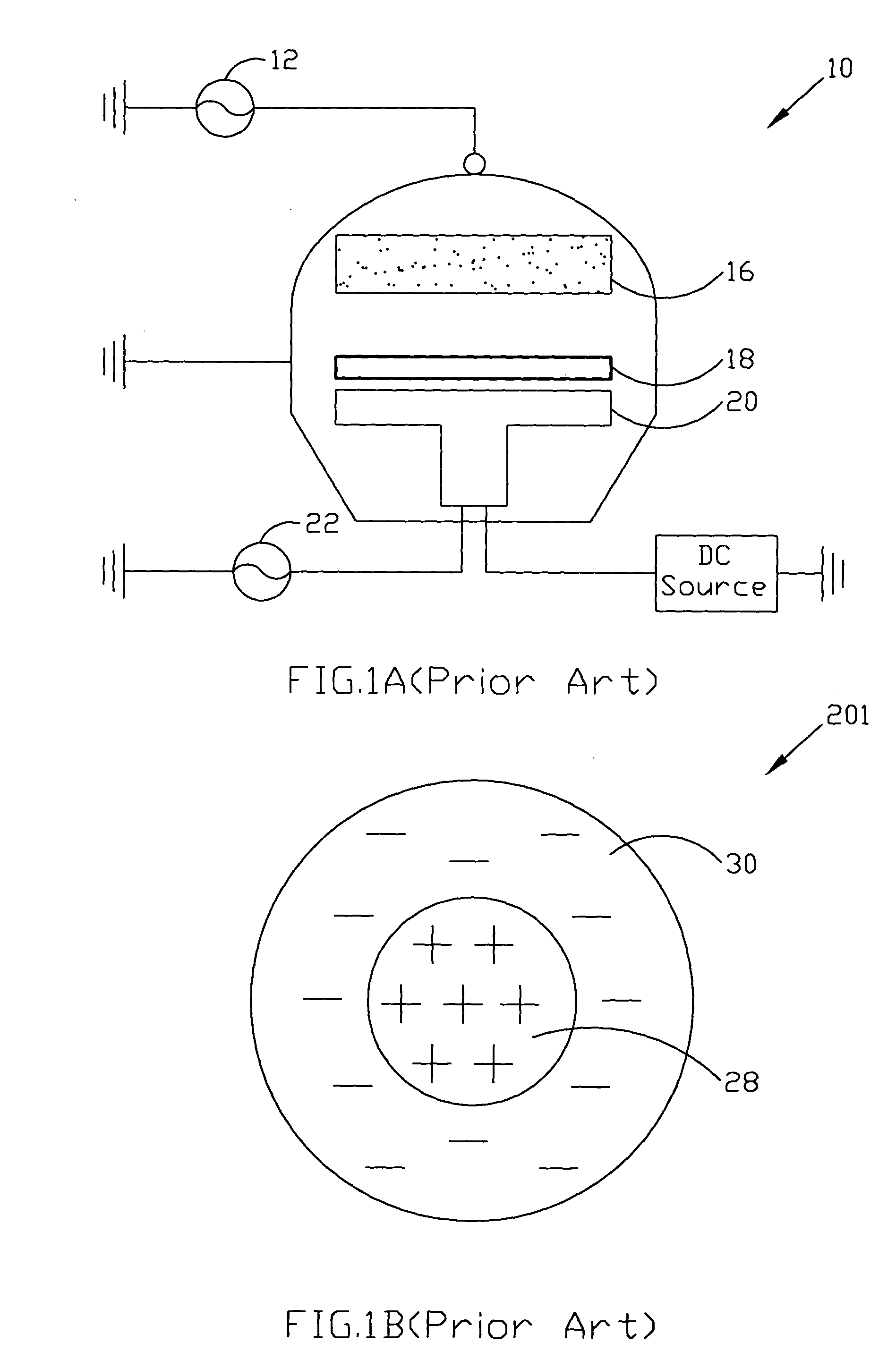
[0022] As shown in FIG. 3A, the apparatus capable of adaptive impedance matching of the present invention mainly applies to HDPCVD equipment. The HDPCVD equipment of the present invention is an inductively-coupled plasma reactor 101. The plasma 16 of high density and low energy is generated by an electromagnetic field produced by AC currents from an AC plasma generating power 12 passing through the inductive coils 14. In the preferred embodiment, the operating frequency of the AC plasma generating power 12 is nearly between 200 KHz and 350 KHz.

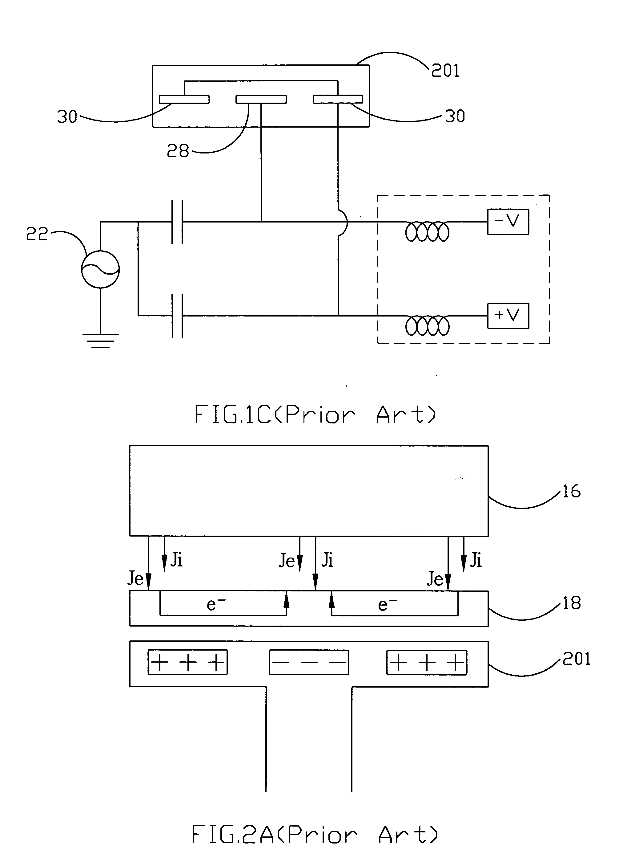
[0023] In HDPCVD process (such as the deposition of inter-metal dielectrics), before proceeding with the deposition ...


PUM

PropertyMeasurementUnit
operating frequencyaaaaaaaaaa
adaptive impedanceaaaaaaaaaa
impedanceaaaaaaaaaa

Abstract

A plasma apparatus capable of adaptive impedance matching comprises a plasma reactor which can produce plasma to proceed with CVD (chemical vapor deposition) process, a bi-polar electrostatic chuck which locates inside the plasma reactor and is used to support and secure a wafer, an alternating current bias power supply which connects to the bi-polar electrostatic chuck supplies the voltage potential bias for ion-bombardment from plasma, and an impedance-matching circuit which connects the alternating current bias power supply to the bi-polar electrostatic chuck is used to balance the inner electrode power output and the outer electrode power output of the bi-polar electrostatic chuck.

Description

BACKGROUND OF THE INVENTION [0001] 1. Field of the Invention [0002] The present invention relates to an apparatus of the fabrication of integrated circuits, and the present invention especially relates to an apparatus of the fabrication of integrated circuits which is capable of reducing gate oxide damage in a high density plasma chemical vapor deposition process to which a bi-polar electrostatic chuck is applied. [0003] 2. Description of the Prior Art [0004] After the fabrication of the active device of a MOS (metal-oxide semiconductor) device is accomplished, the following work is to proceed the fabrication of the multilevel interconnects above the MOS device. As the process technology progresses and scales of MOS devices get more and more smaller, gaps between metal conductors also become more and more narrower. Accordingly, gaps of high aspect ratio between metal conductors are formed. The gaps of high aspect ration will let the deposition of dielectric layers become incomplete ...

Claims


Application Information

Patent Timeline
Patent Type & Authority Applications(United States)
IPC IPC(8): C23C16/458C23C16/507H01J37/32
CPCC23C16/4586C23C16/507Y10T279/23H01J37/32183H01J37/32082
Inventor LAI, CHIEN-HSINLIN, SAN-ANYEN, KUO-ENHUANG, KUO-UEI
Owner MARLIN SEMICON LTD
Why Eureka
Try Eureka