Apparatus for fabricating a high dielectric constant transistor gate using a low energy plasma system

a plasma system and transistor gate technology, applied in the direction of solid-state diffusion coating, vacuum evaporation coating, coating, etc., can solve the problems of increasing the power consumption of the gate, unsatisfactory effects on the performance and durability of the gate, and increasing the leakage current of the ga

Inactive Publication Date: 2007-09-13
APPLIED MATERIALS INC
View PDF20 Cites 30 Cited by
  • Summary
  • Abstract
  • Description
  • Claims
  • Application Information

AI Technical Summary

Problems solved by technology

Attempts have been made to reduce the thickness of SiO2 gate dielectrics below 20 Å. However, it has been found that the use of SiO2 gate dielectrics below 20 Å often results in undesirable effects on gate performance and durability.
Also, there is typically an increase in gate leakage current, i.e., tunneling current, with thin dielectrics that increases the amount of power consumed by the gate.
Thin SiO2 gate dielectrics may be susceptible to NMOS hot carrier degradation, in which high energy carriers traveling across the dielectric can damage or destroy the channel.
Thin SiO2 gate dielectrics may also be susceptible to PMOS negative bias temperature instability (NBTI), wherein the threshold voltage or drive current drifts with operation of the gate.
This may result in a gate leakage reduction, due to tunneling during the operation of a FET, at the same EOT as the un-nitrided oxide dielectric.
As semiconductor devices become smaller, the size of the silicon nitrided gate oxide layer has reached it practical limit.
However, with the further scaling of nitrided silicon dioxide gate dielectric to smaller physical thicknesses (from 10 Å), the gate leakage has increased to unacceptable levels for practical device applications.
Replacement of silicon dioxide (SiO2) with a high-k dielectric type material has presented challenges.
The carbon and other contaminants adversely affect the dielectric properties of the gate dielectric layer.
Also, the quality of the interface between a chemical vapor deposition (CVD) or atomic layer deposition (ALD) deposited high-k film and the channel region is not as robust as a silicon dioxide layer.

Method used


Image

  • Apparatus for fabricating a high dielectric constant transistor gate using a low energy plasma system
  • Apparatus for fabricating a high dielectric constant transistor gate using a low energy plasma system
  • Apparatus for fabricating a high dielectric constant transistor gate using a low energy plasma system

Examples


Embodiment Construction

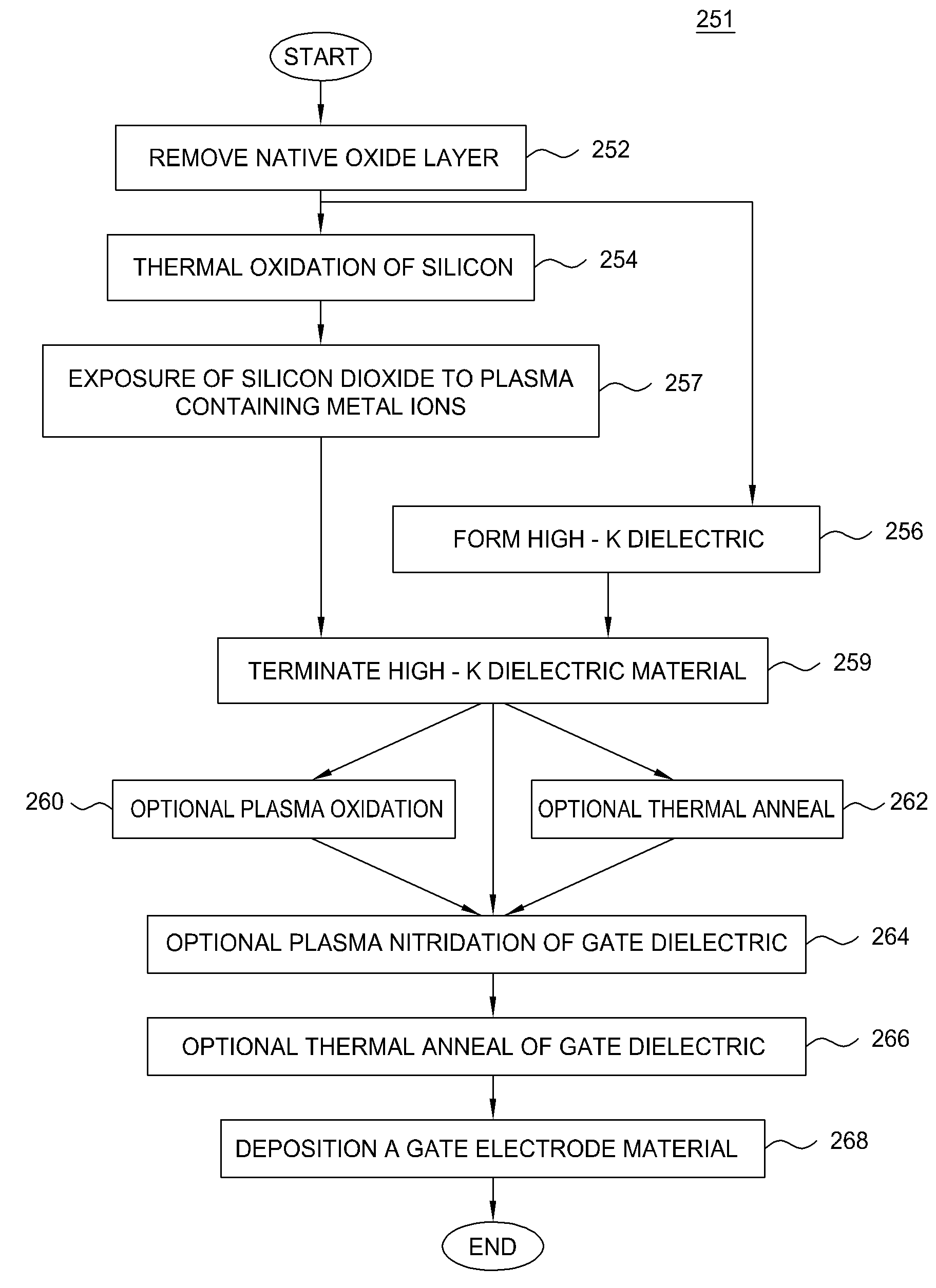
[0042]The present invention generally provides methods and apparatuses that are adapted to form a high quality dielectric gate layer on a substrate. Embodiments contemplate a method wherein a metal plasma treatment process is used in lieu of a standard nitridization process to form a high dielectric constant layer on a substrate. Embodiments further contemplate an apparatus adapted to “implant” metal ions of relatively low energy in order to reduce ion bombardment damage to the gate dielectric layer, such as a silicon dioxide layer, and to avoid incorporation of the metal atoms into the underlying silicon. Embodiments of the invention may be useful in the formation of semiconductor devices, such as logic or memory devices.

Method of Fabricating a High Dielectric Constant Transistor Gate

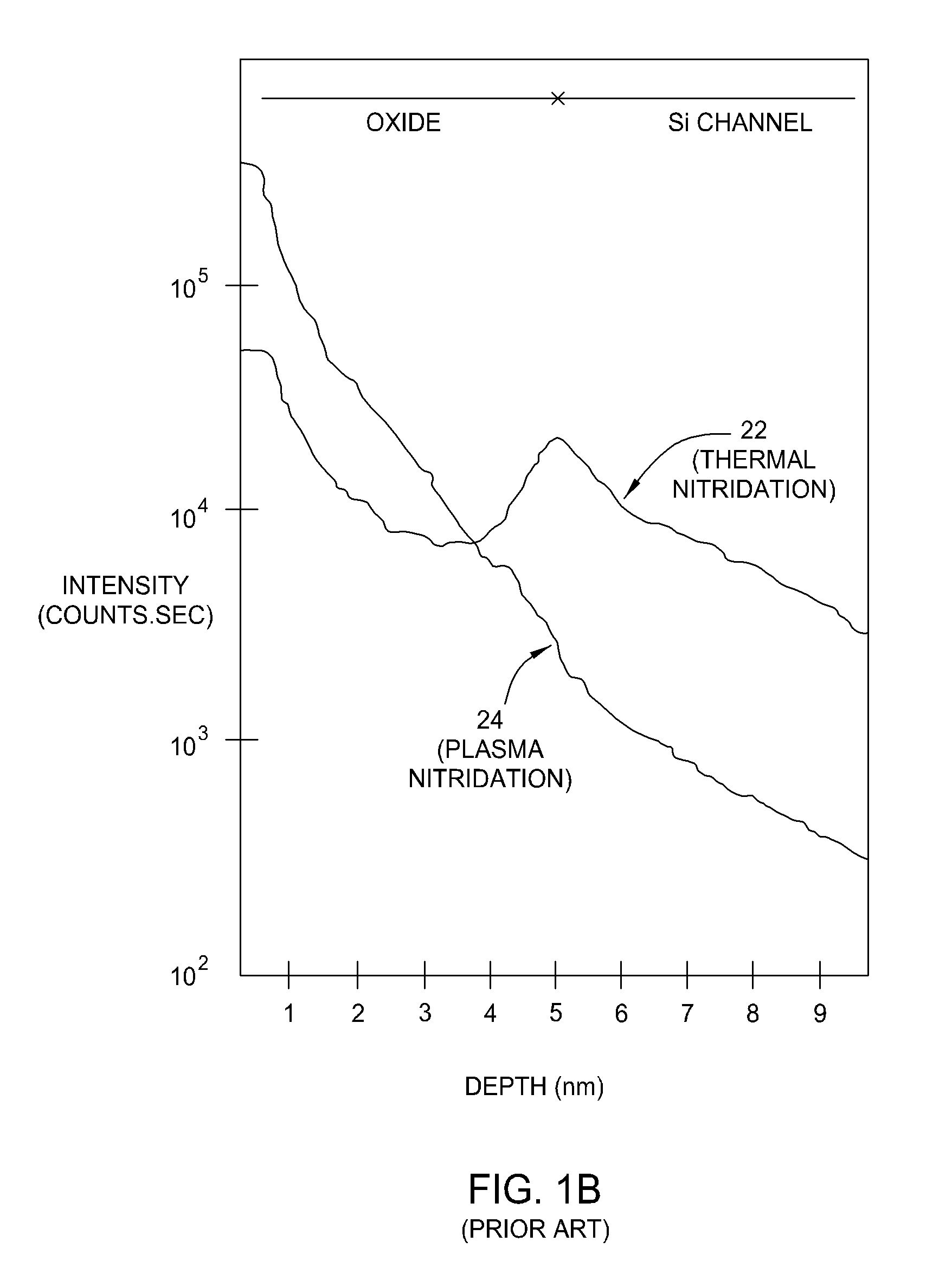
[0043]Current state-of the art device fabrication processes have difficulty in producing a gate dielectric layer that has a 5-10 Å EOT that has a low leakage current. The current state of the art proce...


PUM

PropertyMeasurementUnit
temperatureaaaaaaaaaa
RF frequencyaaaaaaaaaa

Abstract

The present invention generally provides methods and apparatuses that are adapted to form a high quality dielectric gate layer on a substrate. Embodiments contemplate a method wherein a metal plasma treatment process is used in lieu of a standard nitridization process to form a high dielectric constant layer on a substrate. Embodiments further contemplate an apparatus adapted to “implant” metal ions of relatively low energy in order to reduce ion bombardment damage to the gate dielectric layer, such as a silicon dioxide layer and to avoid incorporation of the metal atoms into the underlying silicon. In general, the process includes the steps of forming a high-k dielectric and then terminating the surface of the deposited high-k material to form a good interface between the gate electrode and the high-k dielectric material. Embodiments of the invention also provide a cluster tool that is adapted to form a high-k dielectric material, terminate the surface of the high-k dielectric material, perform any desirable post treatment steps, and form the polysilicon and / or metal gate layers.

Description

CROSS-REFERENCE TO RELATED APPLICATIONS[0001]This application claims benefit of U.S. provisional patent application Ser. No. 60 / 781,508 [APPM 10983L], filed Mar. 9, 2006, which is herein incorporated by reference.BACKGROUND OF THE INVENTION[0002]1. Field of the Invention[0003]Embodiments of the present invention generally relate to a method and an apparatus of forming a high-k dielectric layer. More particularly, embodiments of the invention relate to a method of forming a gate dielectric layer.[0004]2. Description of the Related Art[0005]Integrated circuits are composed of many, e.g., millions, of devices such as transistors, capacitors, and resistors. Transistors, such as field effect transistors, typically include a source, a drain, and a gate stack. The gate stack typically includes a substrate, such as a silicon substrate, a gate dielectric, and a gate electrode, such as polycrystalline silicon, on the gate dielectric. The gate dielectric layer is formed of dielectric materials...

Claims


Application Information

Patent Timeline
Patent Type & Authority Applications(United States)
IPC IPC(8): C23C14/00
CPCC23C8/10C23C8/36C23C14/021C23C14/027C23C14/48H01L21/67207C23C14/5826H01J37/32082H01J37/32146H01J37/32165C23C14/5806
Inventor CHUA, THAI CHENGPATERSON, ALEX M.HUNG, STEVENLIU, PATRICIA M.SATO, TATSUYATODOROW, VALENTINHOLLAND, JOHN P.
Owner APPLIED MATERIALS INC
Why Eureka
Try Eureka