Garbage Collection for Solid State Disks

a solid-state disk and garbage collection technology, applied in the direction of memory architecture accessing/allocation, instruments, electric digital data processing, etc., can solve the problems of not providing full address and data bus capability, not allowing random access to memory locations, and additional bytes of memory, so as to achieve the effect of reducing the number of erasures

Active Publication Date: 2011-01-27
AVAGO TECH INT SALES PTE LTD
View PDF2 Cites 181 Cited by
  • Summary
  • Abstract
  • Description
  • Claims
  • Application Information

AI Technical Summary

Problems solved by technology

However, the I / O interface of NAND flash memory does not provide full address and data bus capability and, thus, generally does not allow random access to memory locations.
As such, the additional bytes of memory are “hidden” from the user and are not available for storing data.
Thus, the direct page mapping scheme requires a large amount of RAM (on the order of 1-2 MB per GB of user storage) to store the translation table, which can become burdensome for higher capacity SSDs.
However, because block mapping does not have a page-level map, the flash media may be inefficiently utilized when the data access workload is non-sequential.
However, because the spare area is used to store page-level mapping information, less memory is available for error correction codes (ECC).
Further, the limited amount of memory available in the spare area precludes storing complicated mapping information.
Finally, reconstruction of the translation table at startup can be time-intensive.
This inefficiency would reduce the realized flash memory capacity because less current data could be stored.
Garbage collection routines impact performance of the flash memory system by utilizing processor resources and potentially delaying write operations to the flash media.
However, NAND device blocks can be erased a limited number of times before device failure (typically on the order of 100,000 erasures).
Therefore, over the operational life of an SSD, blocks of flash memory will fail and become unusable.

Method used


Image

  • Garbage Collection for Solid State Disks
  • Garbage Collection for Solid State Disks
  • Garbage Collection for Solid State Disks

Examples


Embodiment Construction

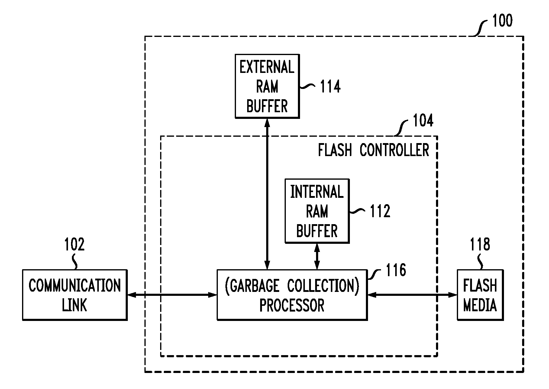
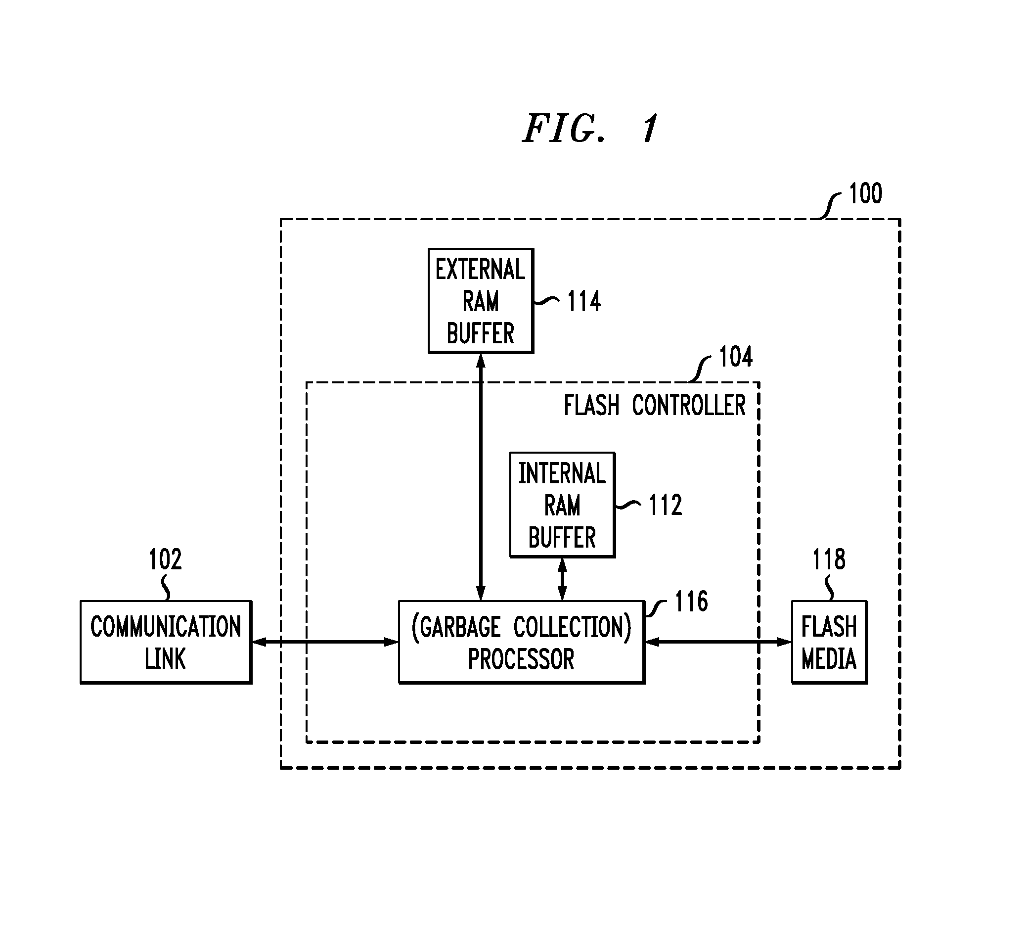
[0026]In accordance with embodiments of the present invention, garbage collection operations for solid state disks (SSDs) are provided. Garbage collection operations allow a flash memory storage system to update a logical memory location by writing data to a new physical memory location without necessarily updating or erasing the previously used physical memory location simultaneously. Garbage collection operations “clean” physical memory locations containing out-of-date or invalid data at a later time. Embodiments of the present invention might provide garbage collection operations to prioritize which blocks to clean in order to minimize the performance impact of garbage collection operations on a given flash memory storage system.

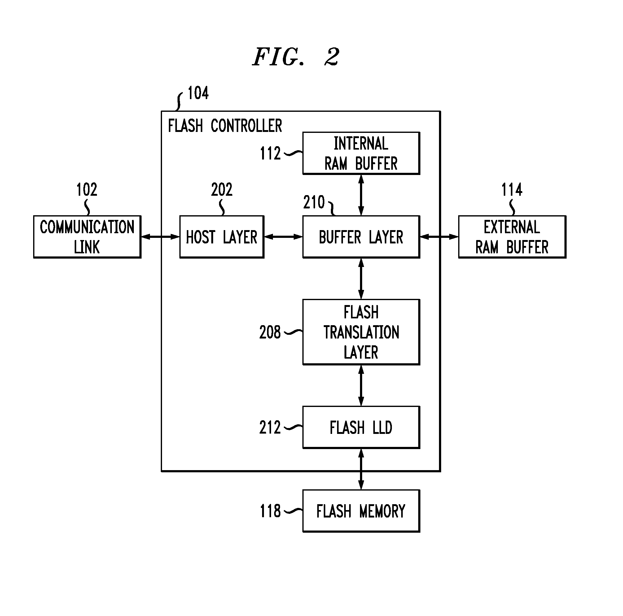
[0027]FIG. 1 shows a block diagram of flash memory storage system 100 implementing a garbage collection routine in accordance with exemplary embodiments of the present invention. As shown, flash memory storage system 100 is electrically coupled to communi...


PUM


Abstract

Described embodiments provide a method of recovering storage space on a solid state disk (SSD). An index and valid page count are determined for each block of a segment of an SSD. If the valid page count of at least one block in the segment is zero, a quick clean is performed. A quick clean deallocates blocks having zero valid pages and places them in a queue for erasure. Otherwise, a deep clean is performed. A deep clean determines a compaction ratio, N-M, wherein N is a number of partially valid blocks and M is a number of free blocks required to compact the valid data from the N partially valid blocks into M entirely valid blocks. At least one data structure of the SSD is modified to refer to the M entirely valid blocks, and the N partially valid blocks are placed in the queue for erasure.

Description

CROSS-REFERENCE TO RELATED APPLICATIONS [0001]The subject matter of this application is related to U.S. patent application Ser. No. 12 / 477,996 filed Jun. 4, 2009, Ser. No. 12 / 478,013 filed Jun. 4, 2009, and Ser. No. 12 / 436,227 filed May 6, 2009, the teachings of all of which are incorporated herein in their entireties by reference.BACKGROUND OF THE INVENTION[0002]1. Field of the Invention[0003]The present invention relates to flash memory storage devices, and, in particular, to garbage collection routines for solid state disks (SSDs).[0004]2. Description of the Related Art[0005]Flash memory is a type of non-volatile memory that is electrically erasable and re-programmable. Flash memory is primarily used in memory cards and USB flash drives for general storage and transfer of data between computers and other digital products. Flash memory is a specific type of electrically erasable programmable read-only memory (EEPROM) that is programmed and erased in large blocks. One commonly empl...

Claims


Application Information

Patent Timeline
Patent Type & Authority Applications(United States)
IPC IPC(8): G06F12/00G06F12/02
CPCG06F2212/7205G06F12/0246G06F2212/1016
Inventor SCHIBILLA, MARK R.REITER, RANDY J.
Owner AVAGO TECH INT SALES PTE LTD
Why Eureka
Try Eureka