Rear-contact solar cell having extensive rear side emitter regions and method for producing the same

Inactive Publication Date: 2011-02-03
INST FUR SOLARENERGIEFORSCHUNG
View PDF9 Cites 41 Cited by
  • Summary
  • Abstract
  • Description
  • Claims
  • Application Information

AI Technical Summary

Benefits of technology

[0013]There may therefore be a need for a rear-contact solar cell and for a method for producing a rear-contact solar cell in which the above-mentioned drawbacks of conventional rear-contact solar cells can be at least partly avoided. In particular, there may be a demand for a rear-contact solar cell which, on the one hand, displays good current-collecting pr

Problems solved by technology

However, the emitter contacts arranged on the front side of the solar cell lead, on account of the partial shading associated therewith of the front side, to a loss in efficiency.
In other words, an unnecessarily large amount of material is deposited on the more extensive emitter contacts when base and emitter contacts are deposited in a common process step.
However, the application of the metal coating for the contacts and also the associated material costs are a considerable portion of the total costs of the solar cells.
However, the formation of a very effectively electrically insulating dielectric layer 209, which is in particu

Method used


Image

  • Rear-contact solar cell having extensive rear side emitter regions and method for producing the same
  • Rear-contact solar cell having extensive rear side emitter regions and method for producing the same
  • Rear-contact solar cell having extensive rear side emitter regions and method for producing the same

Examples


Example

[0064]All the figures are merely schematic and not true-to-scale. In the figures, similar or identical elements are denoted by the same reference numerals.

DETAILED DESCRIPTION OF PREFERRED EMBODIMENTS

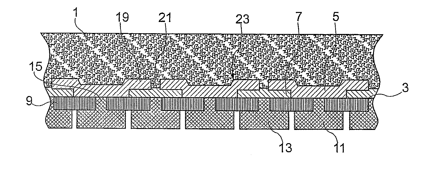
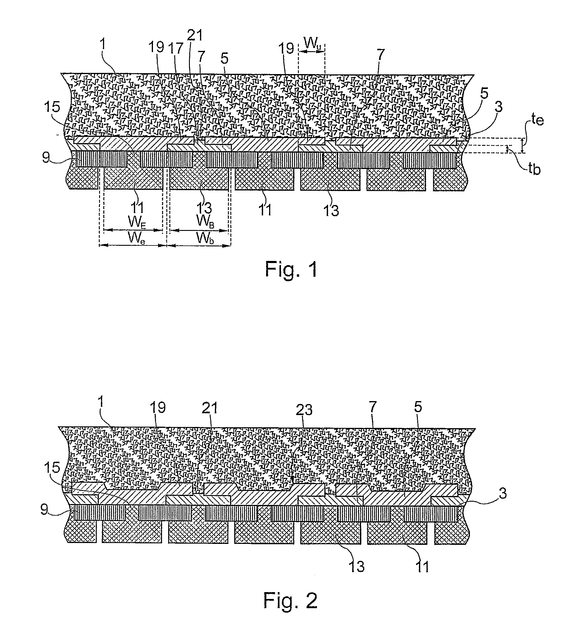
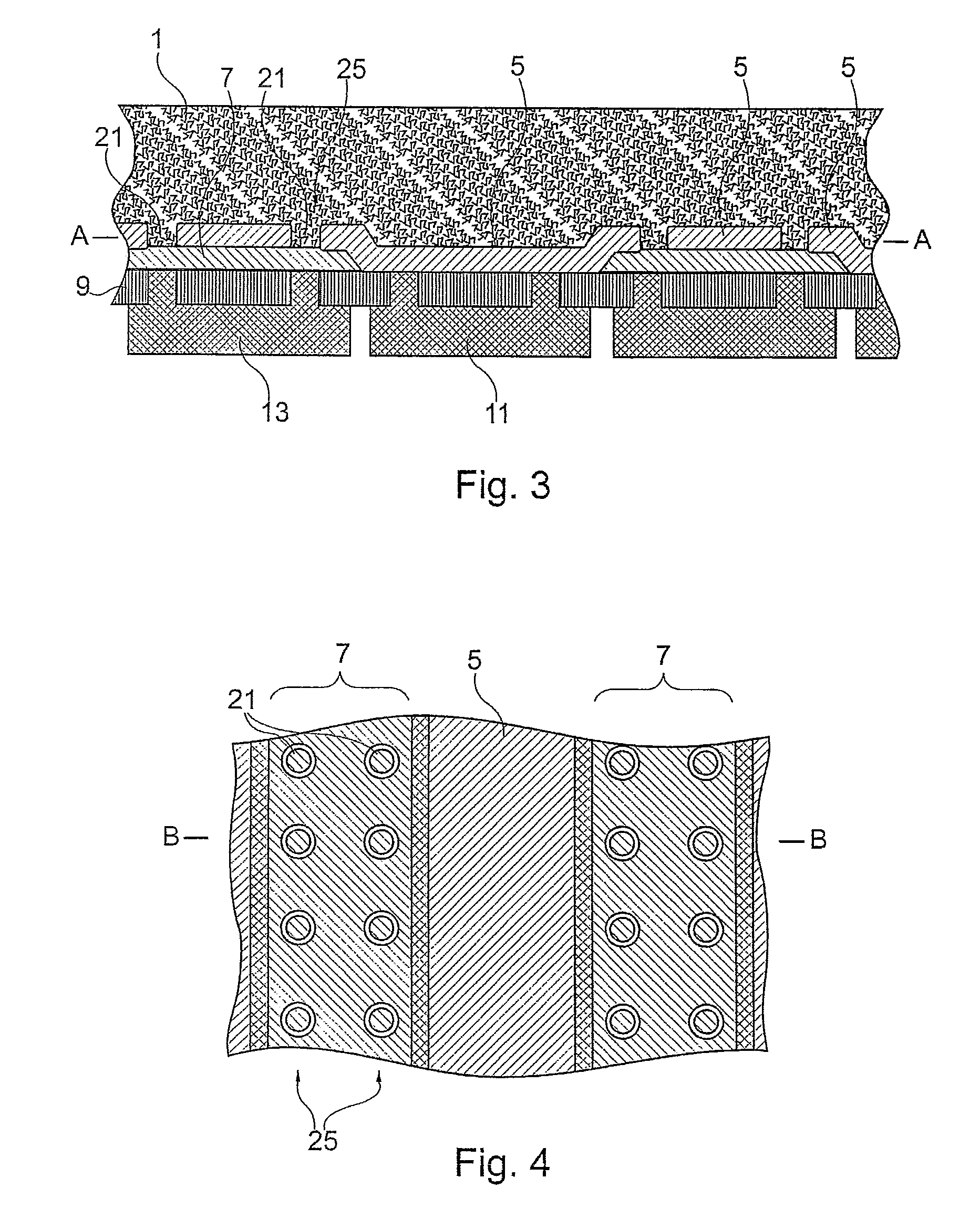
[0065]The rear-contact solar cell according to the invention shown in cross section in FIG. 1 has a semiconductor substrate 1 in the form of a silicon wafer. Both emitter regions 5 and base regions 7 are formed on the rear side surface 3 of the semiconductor substrate 1. A dielectric layer 9 made of silicon oxide or silicon nitride, which can serve to passivate the surface of the semiconductor substrate and / or as a rear side reflector, but does not necessarily have to be electrically insulating, is also located on the rear side surface 3. The emitter contacts 11 and the base contacts 13 are then formed over the dielectric layer 9. Both the emitter and the base contacts 11, 13 are formed in the form of elongate, finger-shaped contacts running perpendicularly to the plane of the drawing. ...


PUM


Abstract

The invention relates to a rear-contact solar cell and to a method for producing the same. The rear-contact solar cell comprises a semiconductor substrate on the rear side surface of which emitter regions, contacted by emitter contacts, and base regions, contacted by base contacts, are defined. The emitter regions and the base regions overlap at least in overlap regions, the emitter regions in the overlap regions reaching deeper into the semiconductor substrate than the base regions, when seen from the rear side surface of the solar cell. As a result, a large area percentage of the rear side of the semiconductor substrate can be covered with a charge-collecting emitter, said emitter being at least partially buried in the interior of the semiconductor substrate so that there is no risk of the base contacts provoking a short circuit towards the buried emitter regions.

Description

FIELD OF THE INVENTION[0001]The present invention relates to a rear-contact solar cell having extensive rear side emitter regions and also to a method for producing a rear-contact solar cell of this type.BACKGROUND TO THE INVENTION[0002]Conventional solar cells have a front side contact, that is to say a contact arranged on a surface of the solar cell that faces the light, and a rear side contact on a surface of the solar cell that is turned away from the light. In these conventional solar cells, the largest volume fraction of a semiconductor substrate absorbing the light is of precisely the semiconductor type (for example p type) which is contacted by the rear side contact. This volume fraction is conventionally referred to as the base and the rear side contacts are therefore conventionally referred to as base contacts. A thin layer of the opposite semiconductor type (for example n type) is located in the region of the surface of the front side of the semiconductor substrate. This ...

Claims


Application Information

Patent Timeline
IPC IPC(8): H01L31/02H01L31/18H01L31/068
CPCH01L31/022441Y02E10/547H01L31/0682
Inventor HARDER, NILS-PETER
Owner INST FUR SOLARENERGIEFORSCHUNG
Why Eureka
Try Eureka