Nano-patterned substrate and epitaxial structure

a substrate and substrate technology, applied in the direction of basic electric elements, electrical equipment, semiconductor devices, etc., can solve the problems of reducing the electron mobility of led, affecting the production yield of subsequent components, and likely affecting the growth of quantum wells, so as to achieve the effect of minimizing defects in the epitaxial structur

Inactive Publication Date: 2011-02-03
EPISTAR CORP +1
View PDF5 Cites 27 Cited by
  • Summary
  • Abstract
  • Description
  • Claims
  • Application Information

AI Technical Summary

Benefits of technology

[0009]The present disclosure provides a nano-patterned substrate rendering minimized defects in an epitaxial structure based on the nano-patterned substrate.
[0010]The present disclosure also provides an epitaxial structure with reduced defects therein.

Problems solved by technology

When the epitaxial growth process is directly applied onto the epitaxial growth surface of the substrate, defects likely occur when the process proceeds to growth of quantum wells.
As a result, not only the production yield of subsequent components is affected, but also the light emitting efficiency and the electron mobility of the LED are reduced.
Therefore, the LED cannot exhibit high light emitting efficiency.

Method used


Image

  • Nano-patterned substrate and epitaxial structure
  • Nano-patterned substrate and epitaxial structure
  • Nano-patterned substrate and epitaxial structure

Examples


first embodiment

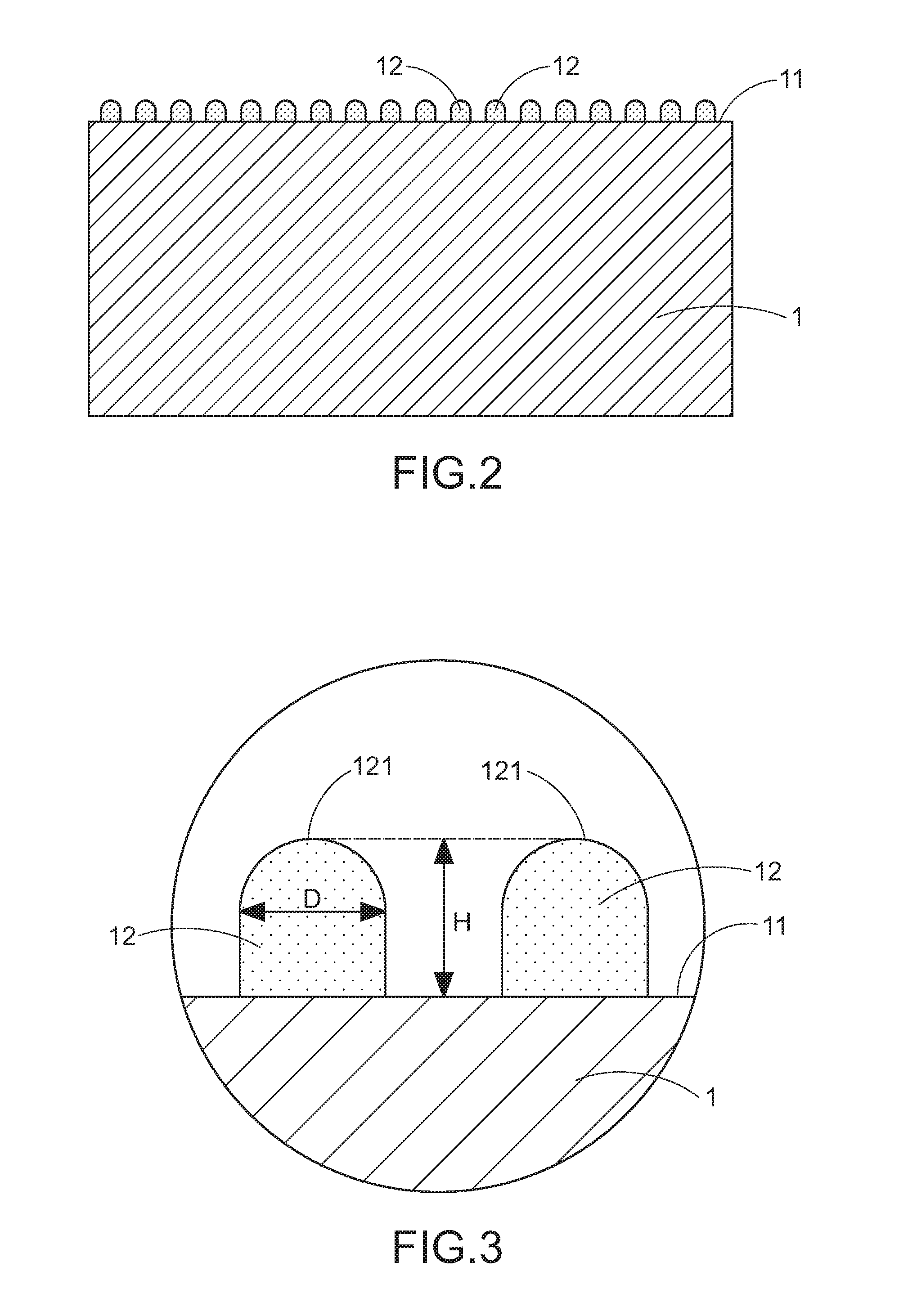
[0027]Referring to FIG. 2, a nano-patterned substrate in accordance with the present disclosure is shown. The nano-patterned substrate 1 includes an upper surface 11. A plurality of nano-particles 12 is disposed on the upper surface 11. Further, referring to FIG. 3, an aspect ratio of each of the nano-particles 12, that is, the ratio of height (H) to diameter (D), is either greater than or equal to 1 (i.e., H / D≧1) and each of the nano-particles 12 has an arc-shaped top surface 121.

[0028]FIG. 4 schematically illustrates a growth process of the nano-patterned substrate in accordance with first embodiment of the present disclosure. Referring to FIG. 4, a buffer layer 21 is formed on the upper surface 11 of the substrate 1. In one embodiment of this disclosure, the material of the buffer layer can be silicon oxide. A metal layer 22 is then formed on the buffer layer 21. A material of the metal layer 22 can be nickel. A thickness of the metal layer 22 is in a range from 50 angstroms to 2...

third embodiment

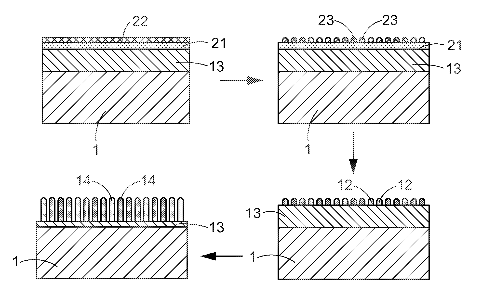
[0030]FIG. 7 illustrates a schematic view of a nano-patterned substrate in accordance with the present disclosure. Referring to FIG. 7, the nano-patterned substrate includes a semiconductor buffer layer 13 disposed on the substrate 1, and a plurality of nanopillors 14 is formed on an upper surface 131 of the semiconductor buffer layer 13. An aspect ratio of the nanopillars 14, that is, the ratio of height (H) to diameter (D) is either greater than or equal to 5 (i.e., H / D≧5). Further, referring to FIG. 8, each of the nanopillars 14 has an arc-shaped top surface 141.

[0031]The formation of the nano-patterned substrate in the third embodiment is similar to the formation of the nano-patterned substrate in the first embodiment. Referring to FIG. 9, the semiconductor buffer layer 13 is formed on the substrate 1. A buffer layer 21 is formed on the semiconductor buffer layer 13. In one embodiment of this disclosure, the material of the buffer layer can be silicon oxide. A metal layer 22 is ...


PUM

PropertyMeasurementUnit
thicknessaaaaaaaaaa
aspect ratioaaaaaaaaaa
temperatureaaaaaaaaaa

Abstract

A nano-patterned substrate includes a plurality of nano-particles or nanopillars on an upper surface thereof. A ratio of height to diameter of each of the nano-particles or each of the nanopillars is either greater than or equal to 1. Particularly, a ratio of height to diameter of the nanopillars is greater than or equal to 5. Each of the nano-particles or each of the nanopillars has an arc-shaped top surface. When an epitaxial growth process is applied onto the nano-patterned substrate to form an epitaxial layer, the epitaxial layer has very low defect density. Thus, a production yield of fabricating the subsequent device can be improved.

Description

CROSS-REFERENCE TO RELATED APPLICATION[0001]This application claims the right of priority based on TW application Ser. No. 098214077, filed Jul. 30, 2009, entitled “NANO-PATTERNED SUBSTRATE AND EPITAXIAL STRUCTURE”, and the contents of which are incorporated herein by reference.BACKGROUND[0002]1. Technical Field[0003]The present disclosure relates to a nano-patterned substrate and an epitaxial structure, and particularly to a nano-patterned substrate and an epitaxial structure of an LED.[0004]2. Description of the Related Art[0005]Compared to a conventional bulb, a light emitting diode (LED) has many advantages like small size, long lifetime, low driving voltage / current, high resistance to damage, low heat accumulation, no pollution from mercury, and high light-emitting efficiency (low power consumption), and so on. Since the light emitting efficiency of LEDs has been increasingly improved, LEDs have been substituting for conventional bulbs such as fluorescent lamps and incandescent...

Claims


Application Information

Patent Timeline
Patent Type & Authority Applications(United States)
IPC IPC(8): H01L29/06H01L21/20
CPCH01L21/02439H01L21/02521H01L21/02603H01L21/02639H01L33/24H01L21/02647H01L33/007H01L33/22H01L21/02645
Inventor LI, ZHEN-YUCHIU, CHING-HUAKUO, HAO-CHUNGLU, TIEN-CHANG
Owner EPISTAR CORP
Why Eureka
Try Eureka