

Substrate structure for cavity package
a technology of substrate structure and cavity, which is applied in the direction of semiconductor devices, semiconductor/solid-state device details, electrical devices, etc., can solve problems such as problems, and achieve the effect of improving the cavity substrate structur
- Summary
- Abstract
- Description
- Claims
- Application Information
AI Technical Summary
Benefits of technology
Problems solved by technology
Method used
Image

Examples
Embodiment Construction
[0001]1. Field of the Invention
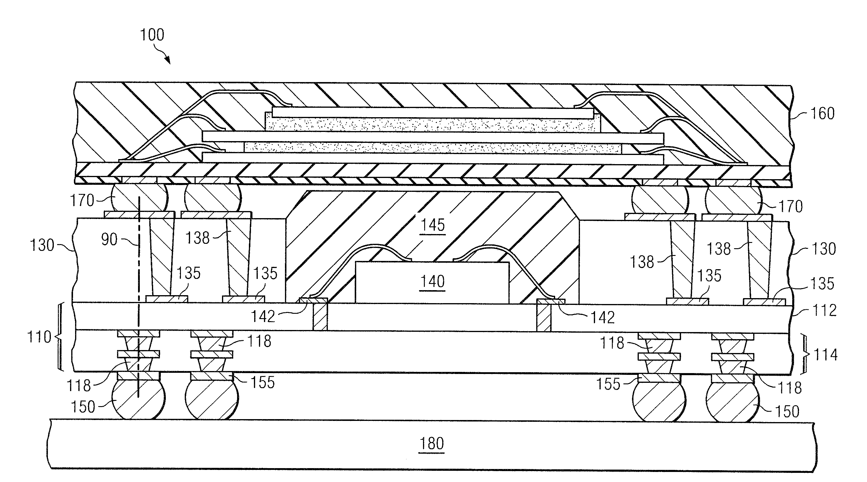
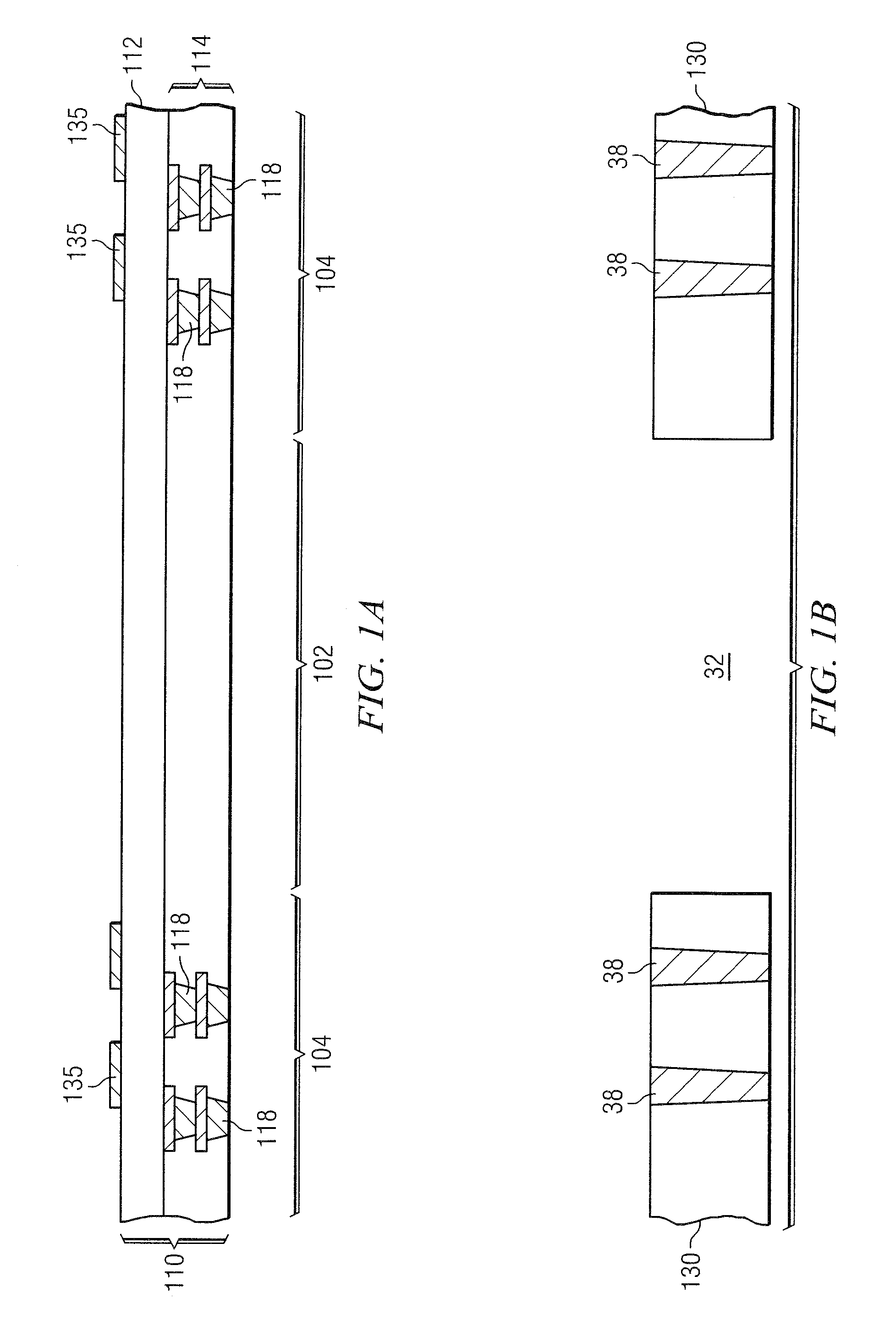
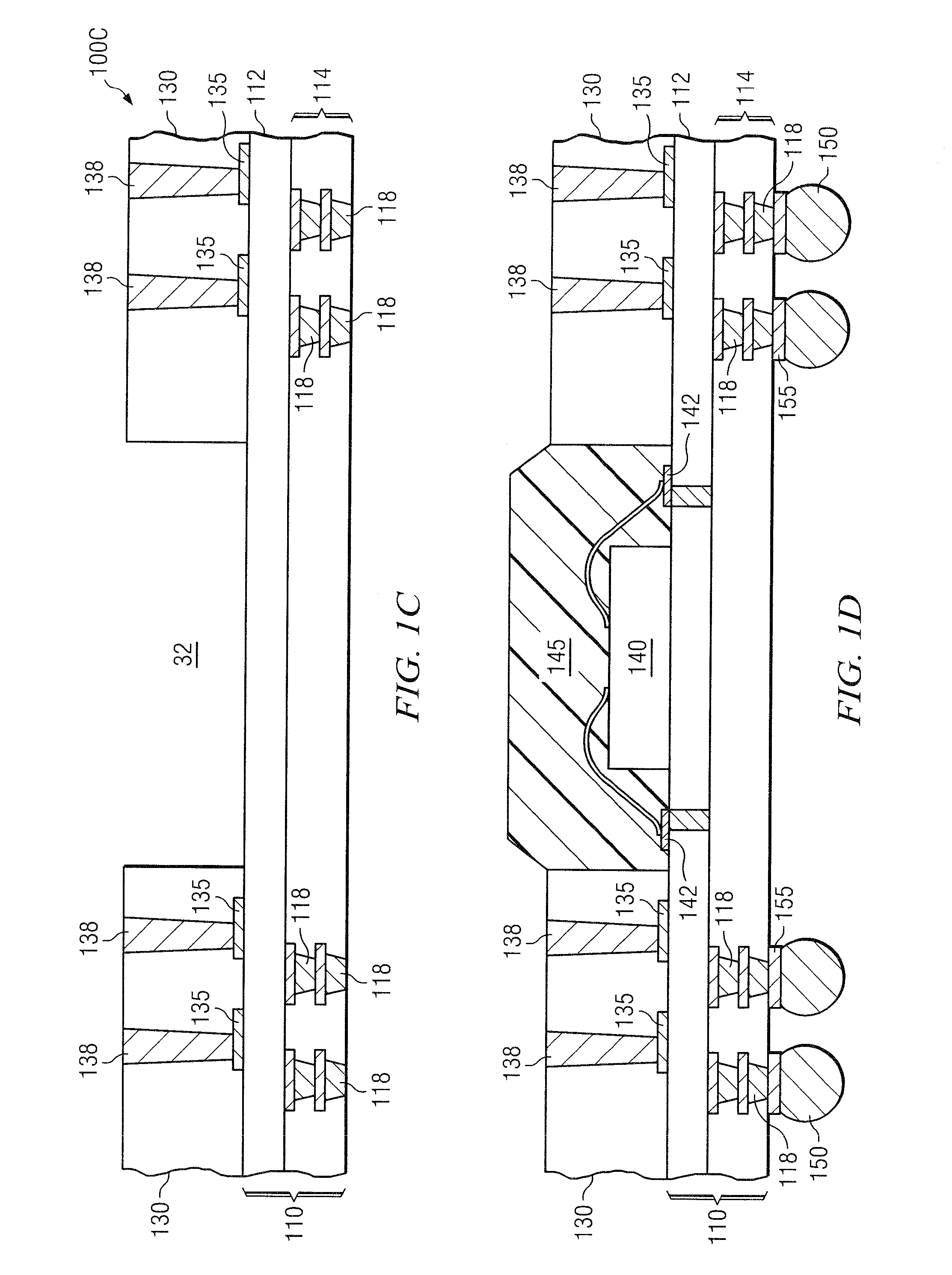
[0002]The invention relates generally to semiconductor device assembly and packaging and, more specifically, to fabricating integrated circuit (IC) devices having three dimensional packaging.
[0003]2. Background of the Invention
[0004]It is well known that the consumers of the next generation electronic devices expect those devices to have increased functions and features that are packed in a smaller size, consume less power, and cost less than previous devices. Semiconductor device manufacturers are responding by incorporating improved three dimensional packaging technologies such as package-on-package (PoP), multi-chip packages (MCPs), systems in package (SiP), as well as others. These packing technologies provide vertical stacking of one or more semiconductor dies and / for packages that are integrated to operate as one semiconductor device. For example, PoP packages are commonly used in products desiring efficient access to memory while reducing size, ...
PUM
 Abstract
Description
Claims
Application Information