Semiconductor light emitting device

a technology of light-emitting devices and semiconductors, which is applied in the direction of semiconductor devices, basic electric elements, electrical appliances, etc., can solve the problems of absorbing light emitted from active layers, reducing light-emitting output, and difficulty in sufficiently inhibiting the generation of lattice defects and cross-shapes, etc., to achieve low driving voltage, low light-emitting output, and low cost

Inactive Publication Date: 2011-02-10
SONY CORP
View PDF2 Cites 2 Cited by
  • Summary
  • Abstract
  • Description
  • Claims
  • Application Information

AI Technical Summary

Benefits of technology

[0007]However, in the foregoing Japanese Unexamined Patent Application Publication No. 2001-267631, the indium composition ratio of AlGaInP or GaInP composing the intermediate layer is set to a significantly small value. Thus, it may be difficult to sufficiently inhibit generation of lattice defect and cross hatch due to lattice mismatching with the GaAs substrate. Thus, in the case where the intermediate layer is provided, it is necessary to set a large indium composition ratio of the intermediate layer for inhibiting generation of lattice defect or the like. However, in the case where the indium composition ratio becomes large, bandgap of the intermediate layer becomes narrow (small), light emitted from an active layer is absorbed, and light emitting output is decreased. Accordingly, a semiconductor light emitting device with a low driving voltage, a high light emitting output, and high reliability has been aspired.
[0013]In the first semiconductor light emitting device and the second semiconductor light emitting device of the embodiments of the invention, the intermediate layer provided between the p-type cladding layer and the contact layer contains the foregoing Ga1-aInaP and has a given thickness, or has the first semiconductor layer containing Ga1-bInbP having a given total thickness. Thereby, voltage drop is kept low, and light emitting output and reliability are able to be improved. In particular, according to the second semiconductor light emitting device of the embodiment of the invention, the intermediate layer has the foregoing super lattice structure including the first semiconductor layer and the second semiconductor layer. Accordingly, the light emitting output is able to be more improved.

Problems solved by technology

Thus, it may be difficult to sufficiently inhibit generation of lattice defect and cross hatch due to lattice mismatching with the GaAs substrate.
However, in the case where the indium composition ratio becomes large, bandgap of the intermediate layer becomes narrow (small), light emitted from an active layer is absorbed, and light emitting output is decreased.

Method used


Image

  • Semiconductor light emitting device
  • Semiconductor light emitting device
  • Semiconductor light emitting device

Examples


first embodiment (

1. First embodiment (example of a semiconductor light emitting device having an intermediate layer between a p-type cladding layer and a p-side contact layer)

2. Modified example (example of other intermediate layer)

second embodiment (

3. Second embodiment (example of other semiconductor light emitting device)

first embodiment

1. First Embodiment

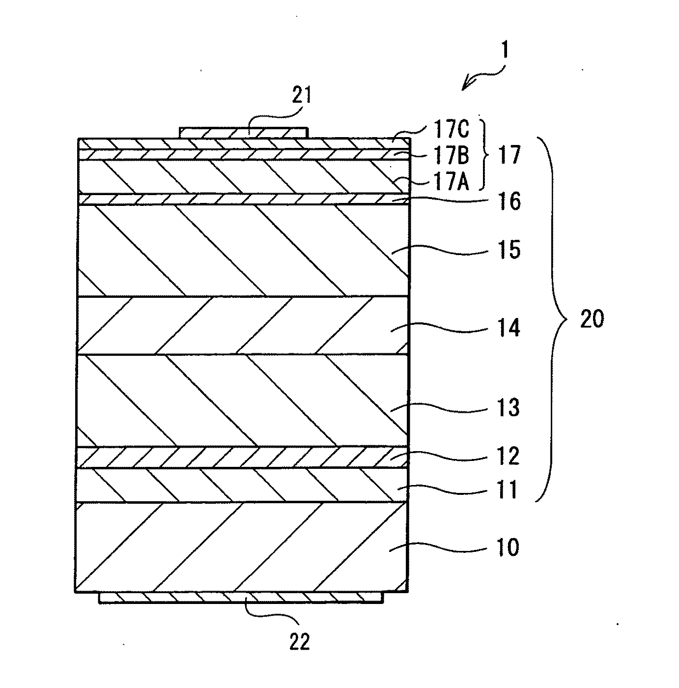
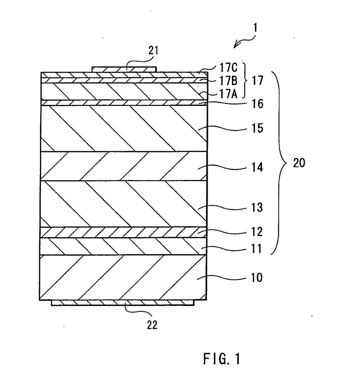
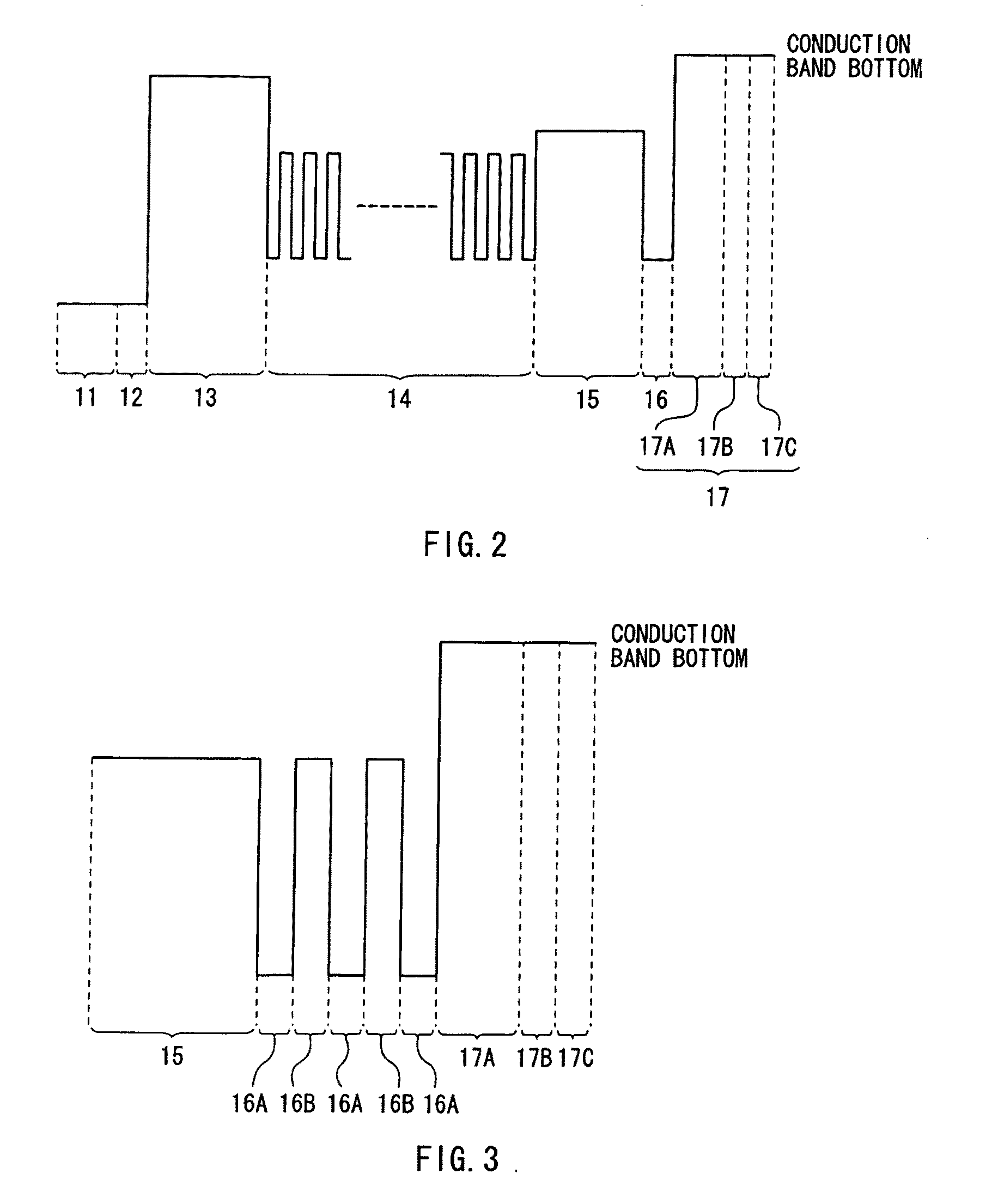
[0022]FIG. 1 schematically illustrates a cross sectional structure of a semiconductor light emitting device according to a first embodiment of the invention. FIG. 2 schematically illustrates a level of conduction band bottom of each energy band in each layer structuring a laminated structure 20 illustrated in FIG. 1. A semiconductor light emitting device 1 in this embodiment includes the laminated structure 20 having an active layer 14 on a substrate 10. A p-side electrode 21 is provided on the laminated structure 20, and an n-side electrode 22 is provided on the rear face side of the substrate 10. In the semiconductor light emitting device 1, light is emitted from the active layer 14. The semiconductor light emitting device 1 is used, for example, as a light emitting diode.

[0023]The laminated structure 20 has a buffer layer 11, an n-side contact layer 12, an n-type cladding layer 13, the active layer 14, a p-type cladding layer 15, an intermediate layer 16, and a...


PUM


Abstract

A semiconductor light emitting device with which a driving voltage is able to be kept low is provided. The semiconductor light emitting device includes: an n-type cladding layer; an active layer; a p-type cladding layer containing AlGaInP; an intermediate layer; and a contact layer containing GaP in this order, wherein the intermediate layer contains Ga1-aInaP (0.357≦a≦0.408), and has a thickness of from 10 nm to 20 nm both inclusive.

Description

BACKGROUND OF THE INVENTION[0001]1. Field of the Invention[0002]The present invention relates to a semiconductor light emitting device having an intermediate layer between a p-type cladding layer and a contact layer.[0003]2. Description of the Related Art[0004]In the past, as a semiconductor light emitting device such as a light emitting diode (LED) that emits light in green to red waveband, AlGaInP semiconductor light emitting devices have been known. Such an AlGaInP semiconductor light emitting device includes, for example, an n-type cladding layer, an active layer, a p-type cladding layer, and a contact layer in this order over a GaAs substrate.[0005]However, in the AlGaInP semiconductor light emitting device, for example, voltage drop is large in a hetero junction between the p-type cladding layer containing AlGaInP and a contact layer containing GaP, and accordingly a voltage for driving the device (driving voltage) is easily increased. Further, lattice defect and a crosshatch ...

Claims


Application Information

Patent Timeline
Patent Type & Authority Applications(United States)
IPC IPC(8): H01L33/34
CPCH01L33/12H01L33/02
Inventor NAGATAKE, TSUYOSHIMITOMO, JUGO
Owner SONY CORP
Why Eureka
Try Eureka