Solid-state imaging device, imaging apparatus, and manufacturing method of solid-state imaging device
- Summary
- Abstract
- Description
- Claims
- Application Information
AI Technical Summary
Benefits of technology
Problems solved by technology
Method used
Image

Examples
first modification
(First Modification)
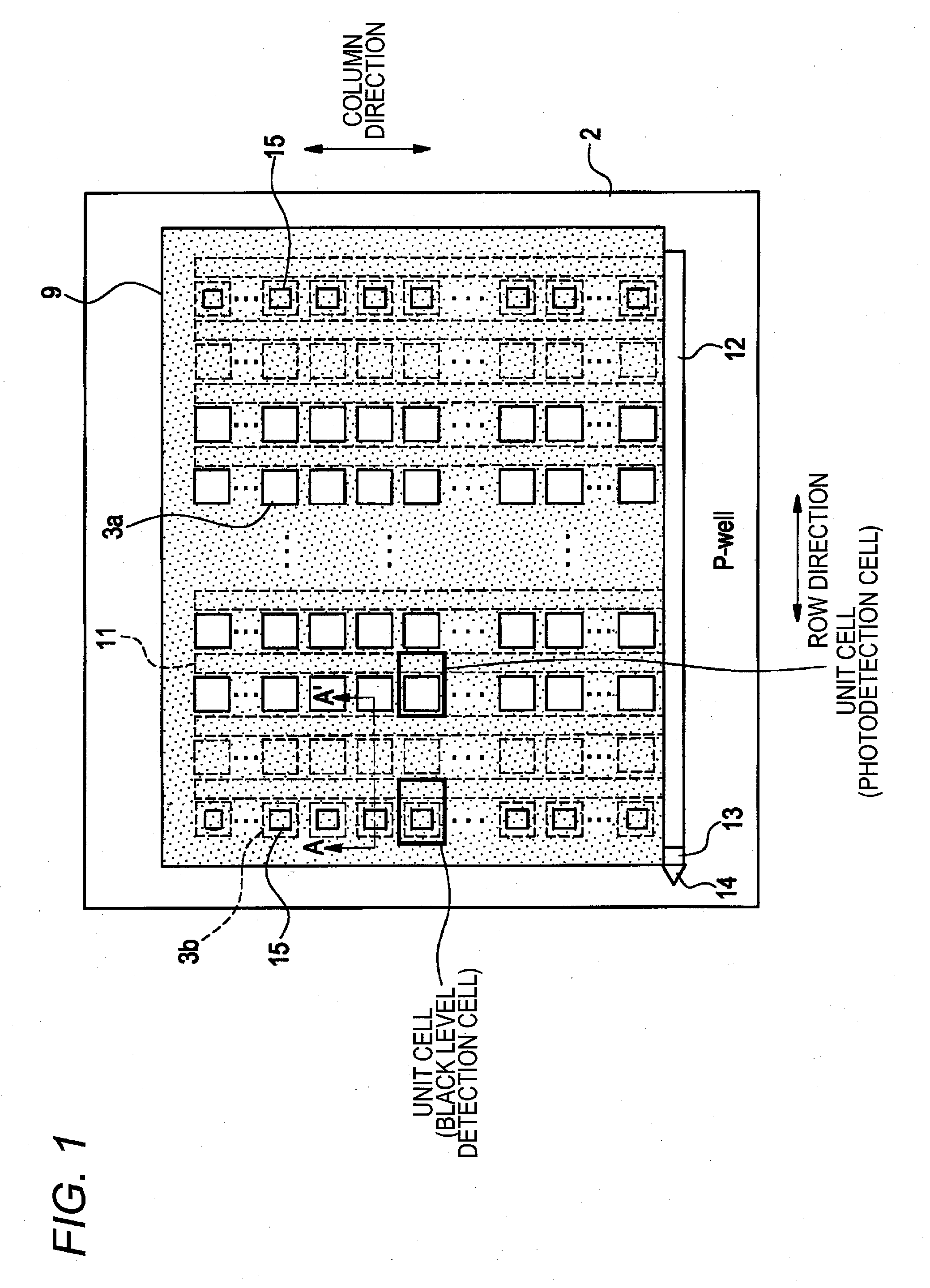
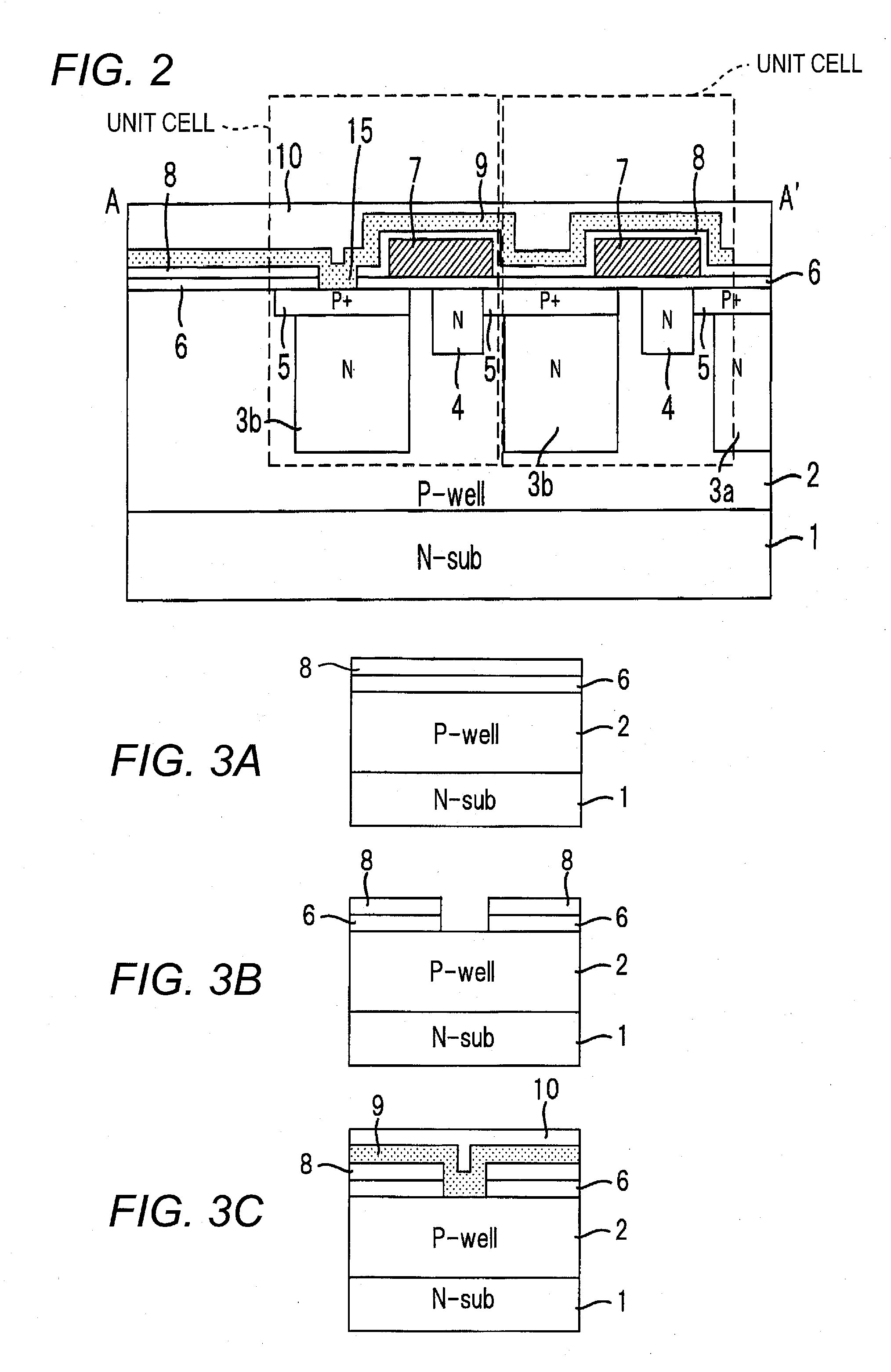
[0057]FIG. 4 shows a first modification of the solid-state imaging device of FIG. 1. The solid-state imaging device of FIG. 4 is different from that of FIG. 1 in that the contact portions 15 of the light shield layer 9 are formed in spaces that are located outside the area where the black level detection cells are formed rather than on the surfaces of the black level detection photoelectric conversion elements 3b. In this case, the contact portions 15 are in contact with the p-well layer through openings formed through the gate insulating layer 6 and the insulating layer 8.
[0058]The manufacturing method of the solid-state imaging device of FIG. 4 is approximately the same as that of the solid-state imaging device of FIG. 1. More specifically, after photodetection cells and black level detection cells are formed in the n-type silicon substrate 1, openings are formed through those parts of the insulating layer 8 and the gate insulating layer 6 which are located in ...
second modification
(Second Modification)
[0062]FIG. 5 shows a second modification of the solid-state imaging device of FIG. 1. Unlike in FIG. 1, the light shield layer 9 is omitted in FIG. 4. FIG. 6 is a schematic sectional view taken along line B-B′ in FIG. 5.
[0063]The solid-state imaging device of FIG. 5 is different from that of FIG. 4 in that p-well layers 16 are formed separately from the p-well layer 2 in spaces that are located outside the area where the black level detection cells are formed. As shown in FIG. 6, the contact portions 15 are in contact with the p-well layers 16 through openings that are formed through the gate insulating layer 6 and the insulating layer 8. Satisfactory results are obtained as long as the contact portions 15 are formed in the vicinity of the black level detection cells. To establish ohmic contact between the p-well layers 16 and the contact portions 15, it is preferable that as shown in FIG. 6 p-type impurity layers be formed adjacent to the surface of each p-well...
PUM
 Abstract
Description
Claims
Application Information
 - R&D Engineer
- R&D Manager
- IP Professional
- Industry Leading Data Capabilities
- Powerful AI technology
- Patent DNA Extraction
Browse by: Latest US Patents, China's latest patents, Technical Efficacy Thesaurus, Application Domain, Technology Topic.
© 2024 PatSnap. All rights reserved.Legal|Privacy policy|Modern Slavery Act Transparency Statement|Sitemap