Physics-based mosfet model for variational modeling

a technology of variational modeling and mosfet, which is applied in the field of physics-based approach to model and optimize metaloxidesemiconductor fieldeffect transistors (mosfet) devices, can solve the problems of limiting the performance of the technology, process variation becomes a major source of yield loss, and the level of variation cannot be avoided

Active Publication Date: 2011-02-17
ORACLE INT CORP
View PDF3 Cites 30 Cited by
  • Summary
  • Abstract
  • Description
  • Claims
  • Application Information

AI Technical Summary

Benefits of technology

In one aspect, one or more embodiments of the present invention relate to a method of optimizing MOSFET device and circuit production including: the definition of key independent parameters, formulating those key independent parameters into a canonical variational form, calculating theoretical extracted parameters using at least one of key independent parameters in canonical variational form, physics-based analytical models, or corner models. The method also includ

Problems solved by technology

As process technology continues to reduce dimensions, process variation becomes a major source of yield loss.
While every effort is made in the fabrication process, and also in the design process, to reduce the magnitude and the impact of these variations, some level of variation can not be avoided and may become a limit

Method used


Image

  • Physics-based mosfet model for variational modeling
  • Physics-based mosfet model for variational modeling
  • Physics-based mosfet model for variational modeling

Examples


Embodiment Construction

Specific embodiments of the present disclosure will now be described in detail with reference to the accompanying Figures. Like elements in the various figures may be denoted by like reference numerals for consistency. Further, in the following detailed description of embodiments of the present disclosure, numerous specific details are set forth in order to provide a more thorough understanding of the invention. However, it will be apparent to one of ordinary skill in the art that the embodiments disclosed herein may be practiced without these specific details. In other instances, well-known features have not been described in detail to avoid unnecessarily complicating the description.

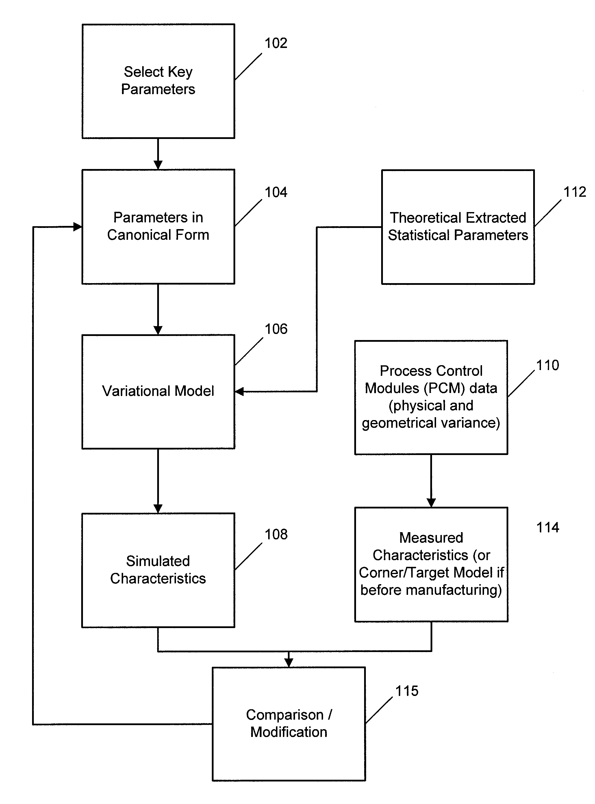
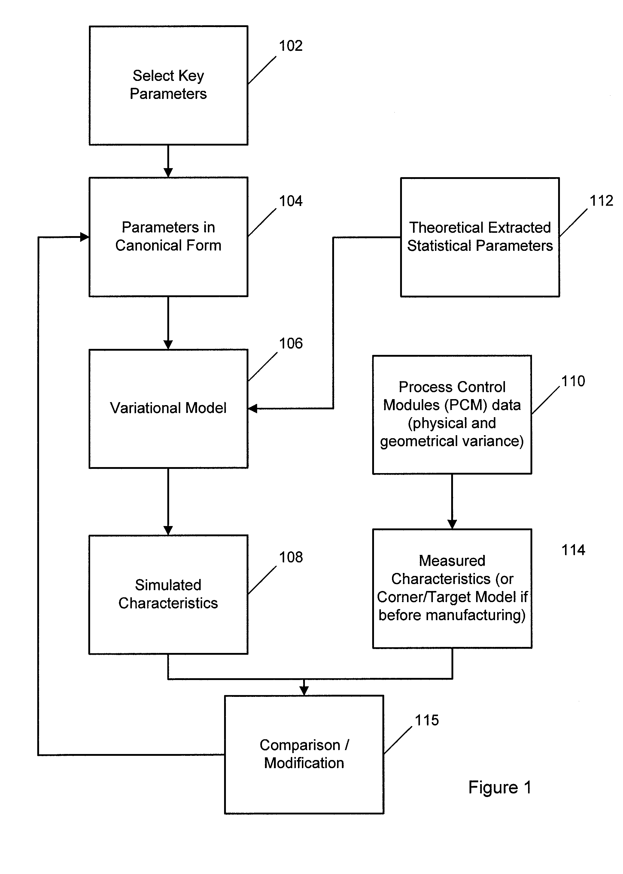
In MOSFET production, as one monitors Lot after Lot, Wafer after Wafer, Die after Die, and Device after Device, a certain natural division becomes apparent. This division allows the system to be broken up into regional domains. In the present application, the first domain is referred to as the Global V...


PUM


Abstract

A method of optimizing MOSFET device production which includes defining key independent parameters, formulating those key independent parameters into a canonical variational form, calculating theoretical extracted parameters using at least one of key independent parameters in canonical variational form, physics-based analytical models, or corner models. The method also includes calculating simulated characteristics of a device using the key independent parameters and extracting target data parameters based on at least one of measured data and predicted data, comparing the simulated characteristics to the target data parameters, and modifying the theoretical extracted parameters or key independent parameters in canonical form as a result of the comparison. Then, calculating and outputting the simulated characteristics based on the modified theoretical extracted parameters and the modified key independent parameters in canonical form.

Description

BACKGROUND OF INVENTION1. Field of the DisclosureEmbodiments described herein generally relate to a physics-based approach to model and optimize metal-oxide-semiconductor field-effect transistor (MOSFET) devices.2. Background ArtAs process technology continues to reduce dimensions, process variation becomes a major source of yield loss. Circuit simulation and timing analysis tools are needed to correctly account for process variations in order to avoid the inherent pessimism of the traditional methodologies and timing analyses. Statistical timing analysis tools have been recently developed to provide more accurate and powerful timing analysis of digital circuits.Inherent equipment and environment fluctuations in the semiconductor fabrication process create a variation in device and circuit performance. While every effort is made in the fabrication process, and also in the design process, to reduce the magnitude and the impact of these variations, some level of variation can not be a...

Claims


Application Information

Patent Timeline
IPC IPC(8): G06F17/50
CPCG06F17/5036G06F30/367
Inventor KHALILY, EBRAHIMBARKER, AARON J.ARDELEA, ALEXANDRU N.
Owner ORACLE INT CORP
Why Eureka
Try Eureka