Method and apparatus for creating an extraction model

a model and extraction method technology, applied in the field of semiconductor design testing, semiconductor manufacturing, semiconductor semiconductors, etc., can solve the problem of decomposing complex extraction problems into smaller, simpler extraction problems, and achieve the effect of high accuracy

Inactive Publication Date: 2006-05-23
CADENCE DESIGN SYST INC
View PDF44 Cites 38 Cited by
  • Summary
  • Abstract
  • Description
  • Claims
  • Application Information

AI Technical Summary

Benefits of technology

[0014]The model creation phase comprises creating one or more extraction models using machine-learning techniques. First, a complex extraction problem is decomposed into smaller simpler extraction problems. Each smaller extraction problem is then analyzed to identify a set of parameters that fully define the smaller extraction problem. Then, models are created using machine learning techniques for all of the smaller simpler extraction problems.
[0015]The machine learning is performed by first creating training data sets composed of the identified parameters from typical examples of the smaller extraction problem and the answers to those example extraction problems as solved using a highly accurate physics based field solver. The training sets are then used to train the models. In one embodiment, neural networks are used to model the extraction problems. To train the neural network models, Bayesian inference is used in one embodiment. Bayesian inference may be implemented with normal Monte Carlo techniques or Hybrid Monte Carlo techniques. After the creation of a set of models for each of the smaller simpler extraction problems, the machine-learning based models may be used for extraction.
[0016]To apply the machine-learning based extraction models, the extraction software first decomposes a larger extraction problem from an integrated circuit layout into the various different smaller simpler extraction problems previously identified. Then, for each smaller simpler extraction problem, the extraction software selects the parameters that define that smaller simpler extraction problem from the integrated circuit layout. The extraction software then supplies the parameters to the machine-learning based extraction model trained for such a smaller simpler extraction problem.

Problems solved by technology

First, a complex extraction problem is decomposed into smaller simpler extraction problems.

Method used


Image

  • Method and apparatus for creating an extraction model
  • Method and apparatus for creating an extraction model
  • Method and apparatus for creating an extraction model

Examples


Embodiment Construction

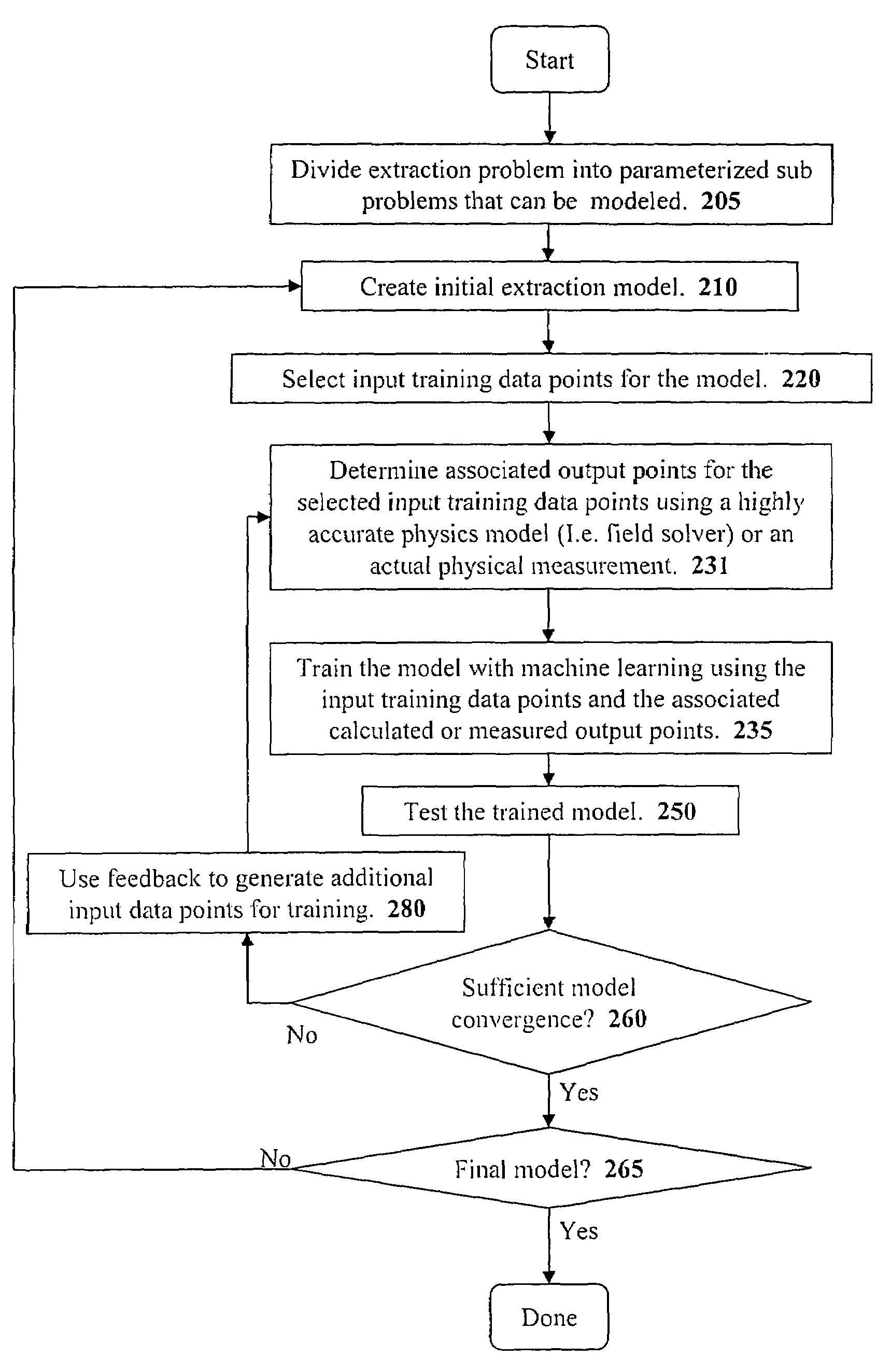
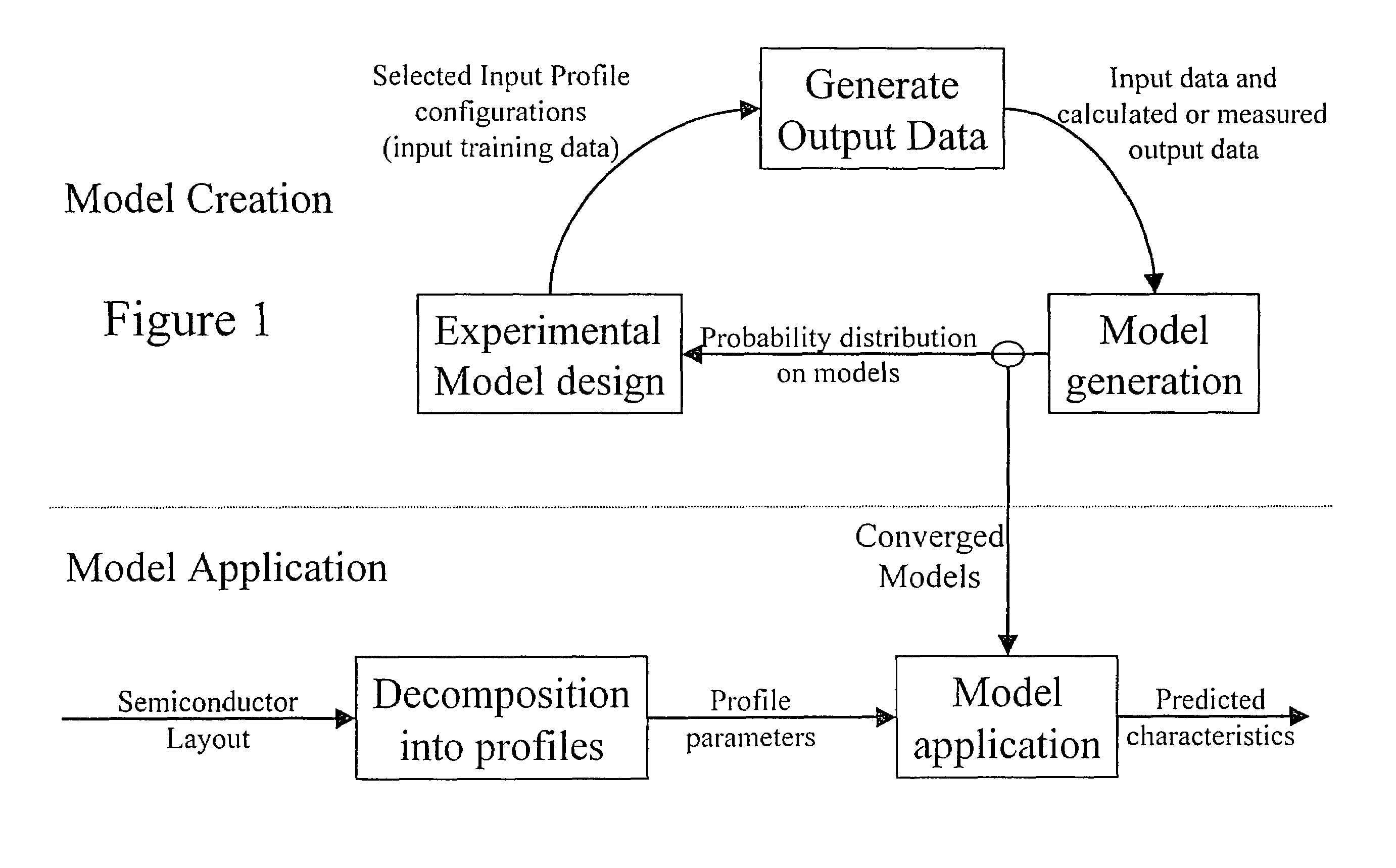
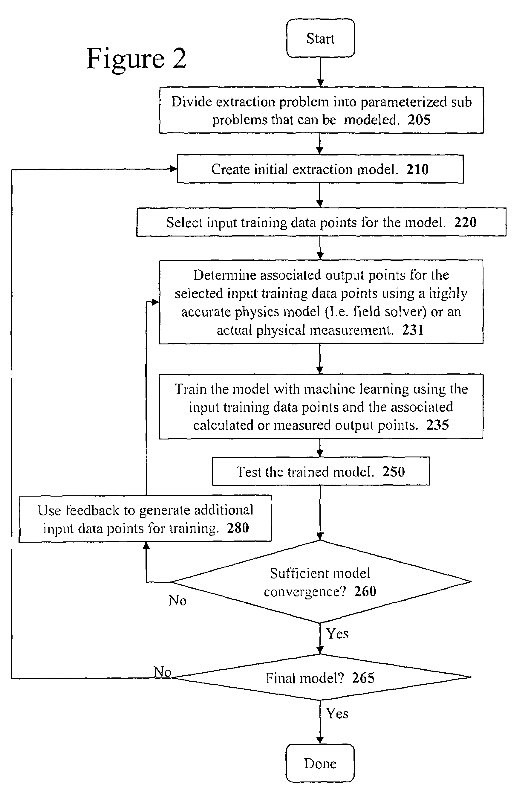
[0051]Methods for extracting electrical characteristics from integrated circuit layouts using probabilistic models are disclosed. In the following description, for purposes of explanation, specific nomenclature is set forth to provide a thorough understanding of the present invention. However, it will be apparent to one skilled in the art that these specific details are not required in order to practice the present invention. For example, the present invention has primarily been described with reference to Bayesian Networks. However, the same techniques can easily be applied to other types of function model creation systems.

Electrical Characteristic Extraction

[0052]Various different methods are used to extract electrical characteristics from an integrated circuit layout. The various different methods have their own advantages and disadvantages.

Field Solvers

[0053]To extract a set of highly accurate electrical characteristics from an integrated circuit layout, an EDA extraction applic...


PUM


Abstract

A system for using machine-learning to create a model for performing integrated circuit layout extraction is disclosed. The system of the present invention has two main phases: model creation and model application. The model creation phase comprises creating one or more extraction models using machine-learning techniques. First, a complex extraction problem is decomposed into smaller simpler extraction problems. Then, each smaller extraction problem is then analyzed to identify a set of physical parameters that fully define the smaller extraction problem. Next, models are created using machine learning techniques for all of the smaller simpler extraction problems. The machine learning is performed by first creating training data sets composed of the identified parameters from typical examples of the smaller extraction problem and the answers to those example extraction problems as solved using a highly accurate physics-based field solver. The training sets are then used to train the models. In one embodiment, neural networks are used to model the extraction problems. To train the neural network models. Bayesian inference is used in one embodiment. Bayesian inference may be implemented with normal Monte Carlo techniques or Hybrid Monte Carlo techniques. After the creation of a set of models for each of the smaller simpler extraction problems, the machine-learning based models may be used for extraction.

Description

[0001]This application claims benefit of applications 60 / 315,867 and 60 / 315,834 both filed Aug. 28, 2001.FIELD OF THE INVENTION[0002]The present invention relates to the field of semiconductor design, semiconductor design testing, and semiconductor manufacture. In particular the present invention discloses methods for estimating various electrical and physical properties of semiconductor integrated circuit designs.BACKGROUND OF THE INVENTION[0003]Complex digital integrated circuits (“ICs”) are initially designed using high-level logic elements such as adders, arithmetic / logic units (ALUs), memory units, buses, etc. These high level elements are in turn constructed from lower level components such as AND gates, OR gates, inverters, etc. These lower level components are constructed from basic electronic components such as transistors, diodes, and electrical conductive traces. All of these electronic and circuit components of ICs are jointly referred to as “components.”[0004]Design eng...

Claims


Application Information

Patent Timeline
Patent Type & Authority Patents(United States)
IPC IPC(8): G06F17/50
CPCG06F17/5081G06F17/5068G06F30/39G06F30/398
Inventor TEIG, STEVENCHATTERJEE, ARINDAM
Owner CADENCE DESIGN SYST INC
Why Eureka
Try Eureka