Flexible semiconductor device and method for manufacturing the same

a technology of flexible semiconductors and semiconductors, applied in the direction of semiconductor devices, electrical equipment, transistors, etc., can solve the problems of peeling step of the substrate, lack of flexibility and breakage, and high price of the display panel, and achieve good densification properties, good smoothness, and thin thickness

Active Publication Date: 2011-02-24
PANASONIC INTELLECTUAL PROPERTY MANAGEMENT CO LTD
View PDF13 Cites 30 Cited by
  • Summary
  • Abstract
  • Description
  • Claims
  • Application Information

AI Technical Summary

Benefits of technology

[0041]According to the manufacturing method of the present invention, the metal foil is subjected to an oxidation treatment at the surface area thereof to form the metal oxide film. The resulting oxide film is used as a gate insulating film. Accordingly, in the present invention, the gate insulating film with a thin thickness and its good densified property (i.e. good smoothness) is obtained, which leads to an achievement of the outstanding TFT performances of the flexible semiconductor device.
[0042]Moreover, “non-oxidized portion” formed by the local oxidation treatment of the metal foil is used as a via. Due to the via having a form of “non-oxidized portion”, a connection among the layers (interlayer connection) can be simply and easily realized without a complicated configuration of the flexible semiconductor device. In addition, it is also unnecessary to remove some parts of the insulating layer after the formation thereof. That is, there is needed no further process for removing the densified and chemically stabilized metal oxide film. Therefore, the raw materials and the energy can be utilized without a wasting thereof, which leads to an achievement of excellent productivity in the manufacturing method of the present invention.
[0043]Moreover, according to the present invention, the metal foil, which has been used as a raw material of the metal oxide film (namely, a raw material for “gate insulating film”), is used as the constituent material of the electrodes i.e. the constituent element of the flexible semiconductor device. Consequently, a high temperature process can be positively employed upon the production of the insulating film and the semiconductor layer. This means that the heat treatment can be positively performed for example during or after the formation of the semiconductor layer, and thereby the TFT characteristics (e.g. carrier mobility of the semiconductor) are desirably improved. In other words, the flexible semiconductor device obtained according to the manufacturing method of the present invention has a high performance with respect to the TFT characteristics, due to the desired heat treatment upon the manufacturing thereof.

Problems solved by technology

However a quartz substrate is so expensive that an economical problem arises when scaling up of the display panels.
However, when the thin display panel as described above is produced by using the conventionally known glass substrate, there is a possibility that such display panel has a heavy weight, lacks flexibility and breaks due to a shock when it is fallen down.
These problems, which are attributable to the formation of a TFT element on a glass substrate, are so undesirable in light of the needs for a portable thin display having light weight with the advancement of informatization.
In the method for manufacturing a TFT element using such a transference process, there is, however, a problem in the peeling step of the substrate (i.e. glass substrate).
These additional treatments make the process complicated, so that another problem concerning productivity is caused.

Method used


Image

  • Flexible semiconductor device and method for manufacturing the same
  • Flexible semiconductor device and method for manufacturing the same
  • Flexible semiconductor device and method for manufacturing the same

Examples


Embodiment Construction

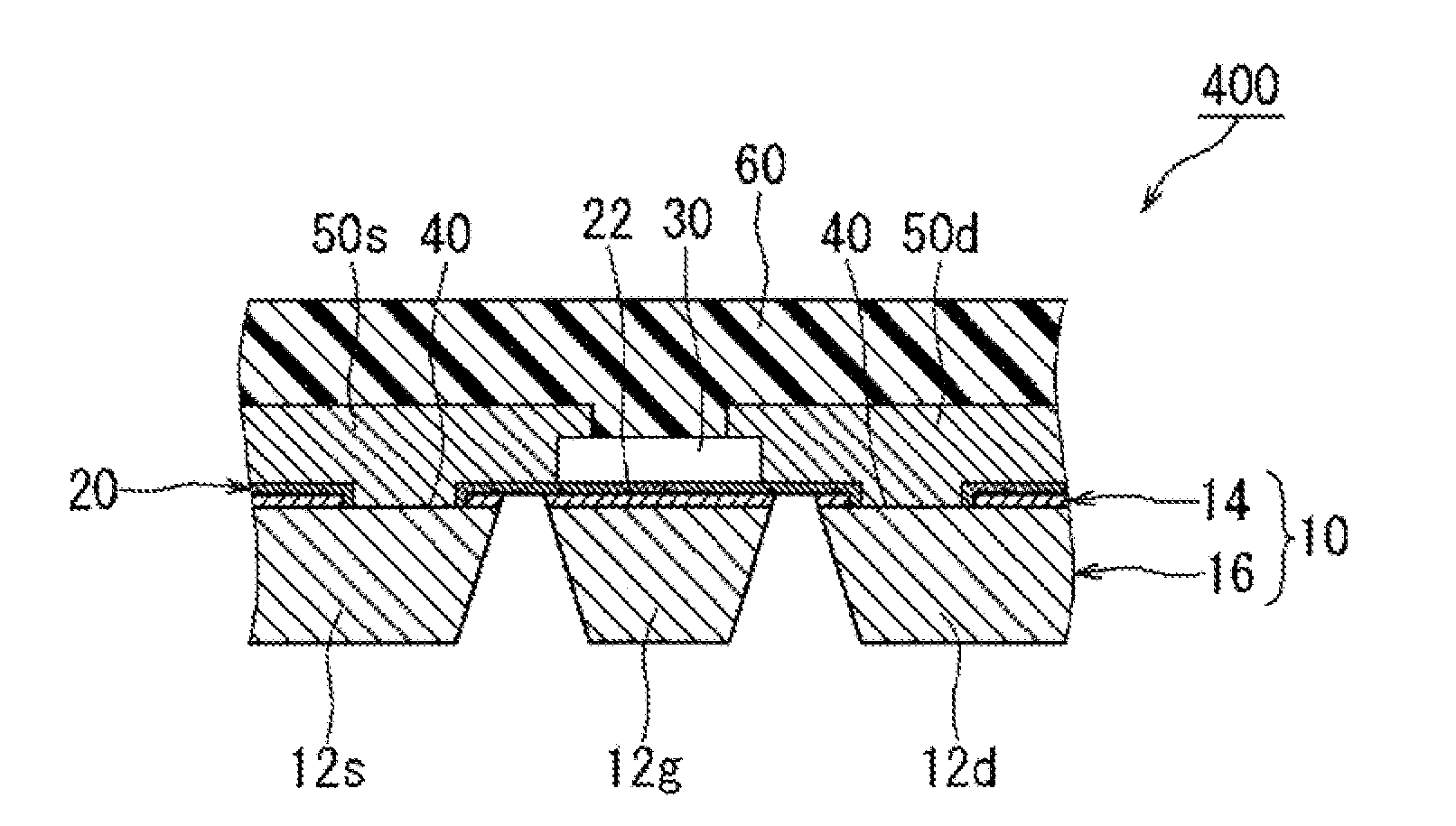
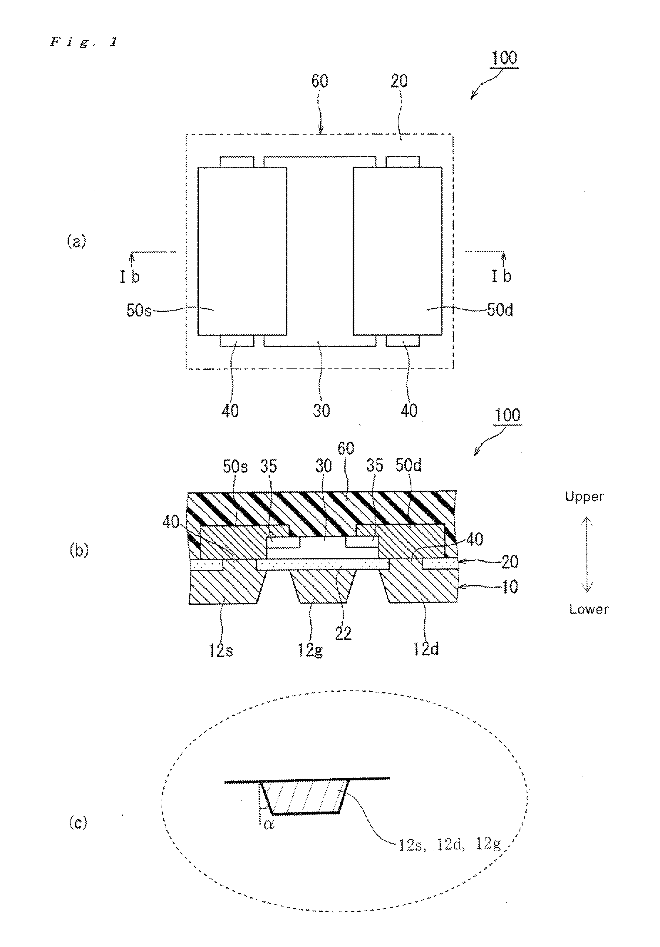
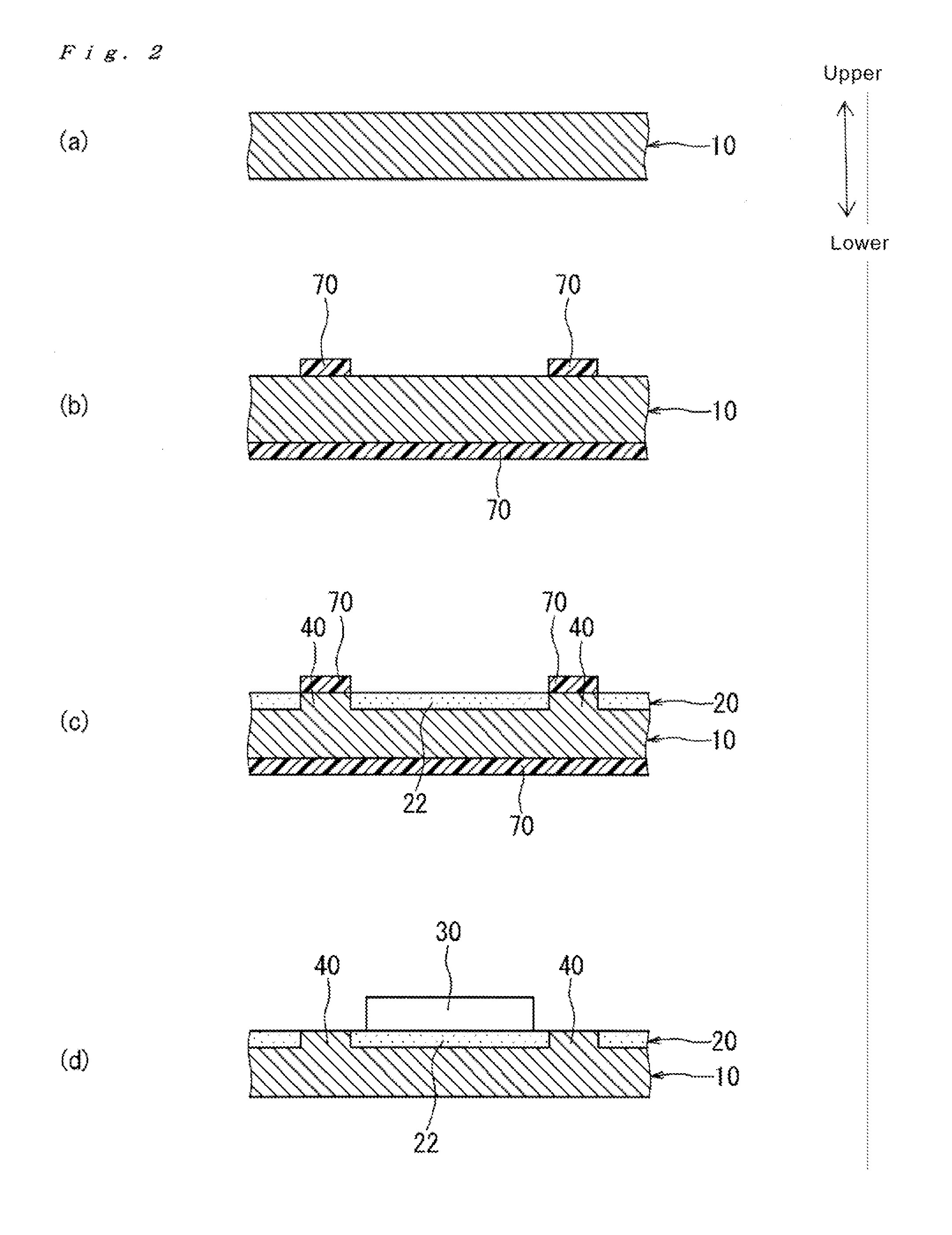
[0065]Hereinafter, some embodiments of the present invention are illustrated with reference to Figures. In the following Figures, the same reference numeral indicates the element which has substantially the same function for simplified explanation. The dimensional relationship (length, width, thickness and so forth) in each Figure does not reflect a practical relationship thereof.

[0066]Each “direction” referred to in the present description means the direction based on the spacial relationship between the metal foil / metal layer 10 and the semiconductor layer 30, in which each of upward direction and downward direction is mentioned relating to the direction in the drawings for convenience. Specifically, each of upward direction and downward direction corresponds to the upward direction and downward direction in each drawing. The side on which the gate insulating film 22 or the semiconductor layer 30 is formed based on the metal foil / metal layer 10 is referred to as “upward direction”...


PUM

PropertyMeasurementUnit
thicknessaaaaaaaaaa
temperatureaaaaaaaaaa

Abstract

There is provided a flexible semiconductor device. The flexible semiconductor device of the present invention comprises a metal layer comprising a gate electrode, a source electrode and a drain electrode; a metal oxide film made from a metal which constitutes the metal layer and formed over a surface region of the metal layer; and a semiconductor layer formed above the gate electrode via the metal oxide film. In the flexible semiconductor device, uncovered portions, each of which is not covered with the metal oxide film, are locally formed in the surface region of the metal layer; and also electrical connections are formed between the source electrode and the semiconductor layer and between the drain electrode and the semiconductor layer via the uncovered portions.

Description

TECHNICAL FIELD[0001]The present invention relates to a flexible semiconductor device with its flexibility, and also a method for manufacturing the same. In particular, the present invention relates to the flexible semiconductor device which can be used as a TFT, and also the method for manufacturing the same.BACKGROUND OF THE INVENTION[0002]There is a growing need for a flat-panel display as an image display device with a wide spreading use of information terminals. With further advancement of informatization, there are also increasing opportunities in which information, which has been conventionally provided by paper medium, is digitized. Particularly, the needs for an electronic paper or a digital paper have been recently increasing since they are thin and light weight mobile display media which can be easily held and carried (see Patent document 1, described below).[0003]Generally, the display medium of a flat panel display device is formed by using an element such as a liquid c...

Claims


Application Information

Patent Timeline
Patent Type & Authority Applications(United States)
IPC IPC(8): H01L33/08H01L21/336
CPCH01L29/66742H01L29/66765H01L29/7869H01L29/78603H01L29/78681H01L29/786
Inventor SUZUKI, TAKESHIHOTEHAMA, KENICHIHIRANO, KOICHINAKATANI, SEIICHI
Owner PANASONIC INTELLECTUAL PROPERTY MANAGEMENT CO LTD
Why Eureka
Try Eureka