According to the present invention, disadvantages and problems associated with previous solutions for altering the rate of thermal expansion of a substrate may be reduced or eliminated.
In certain embodiments, a method includes forming a composite
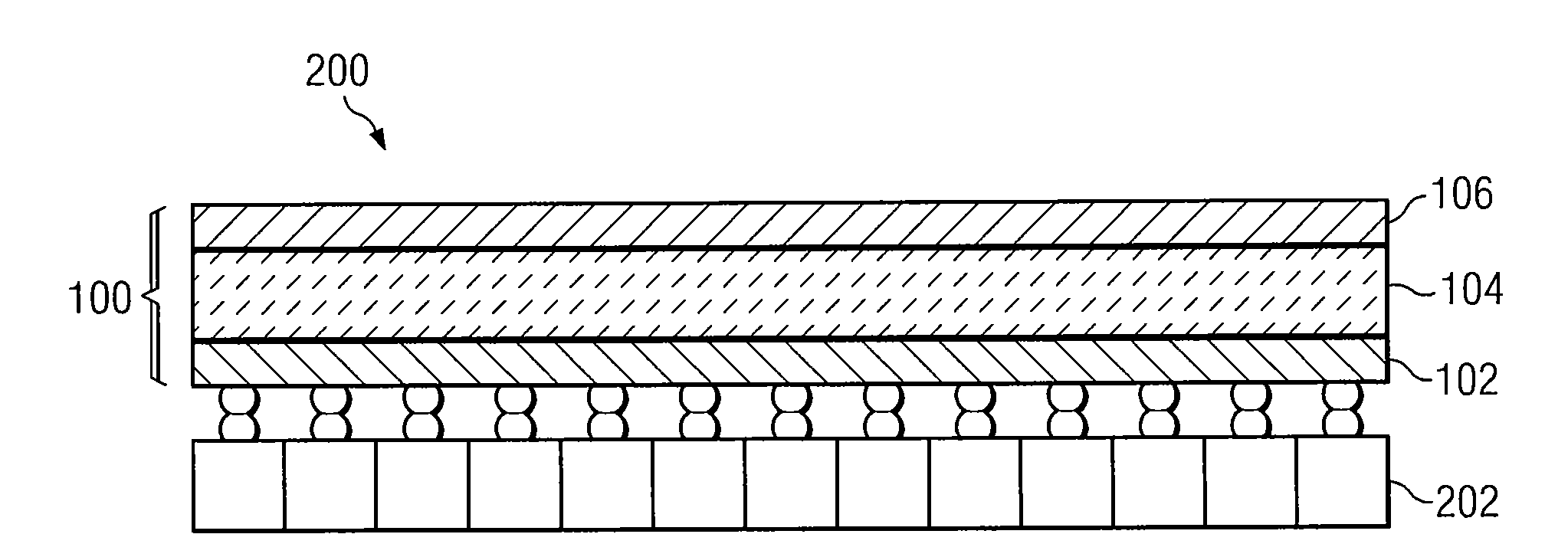
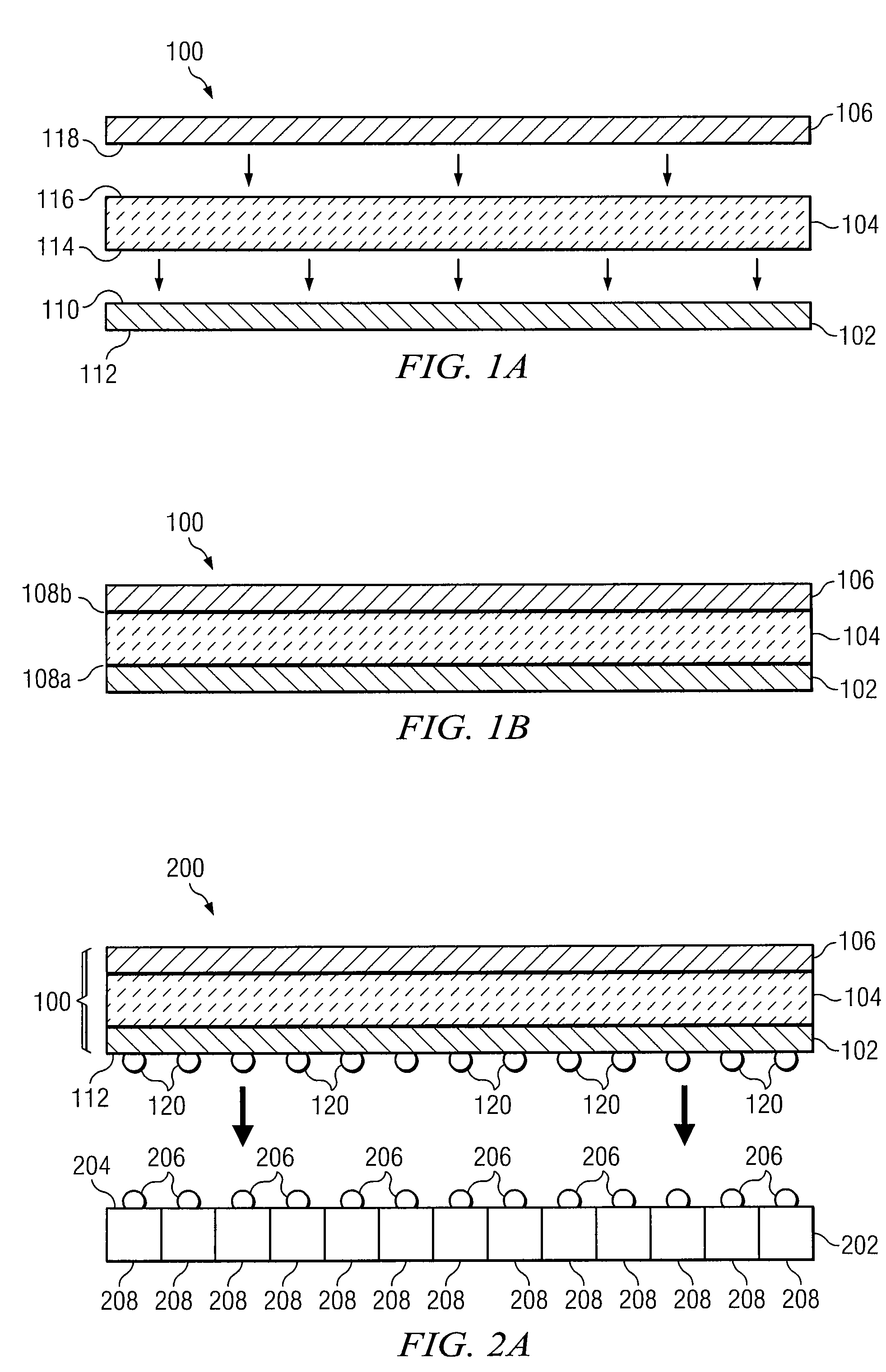
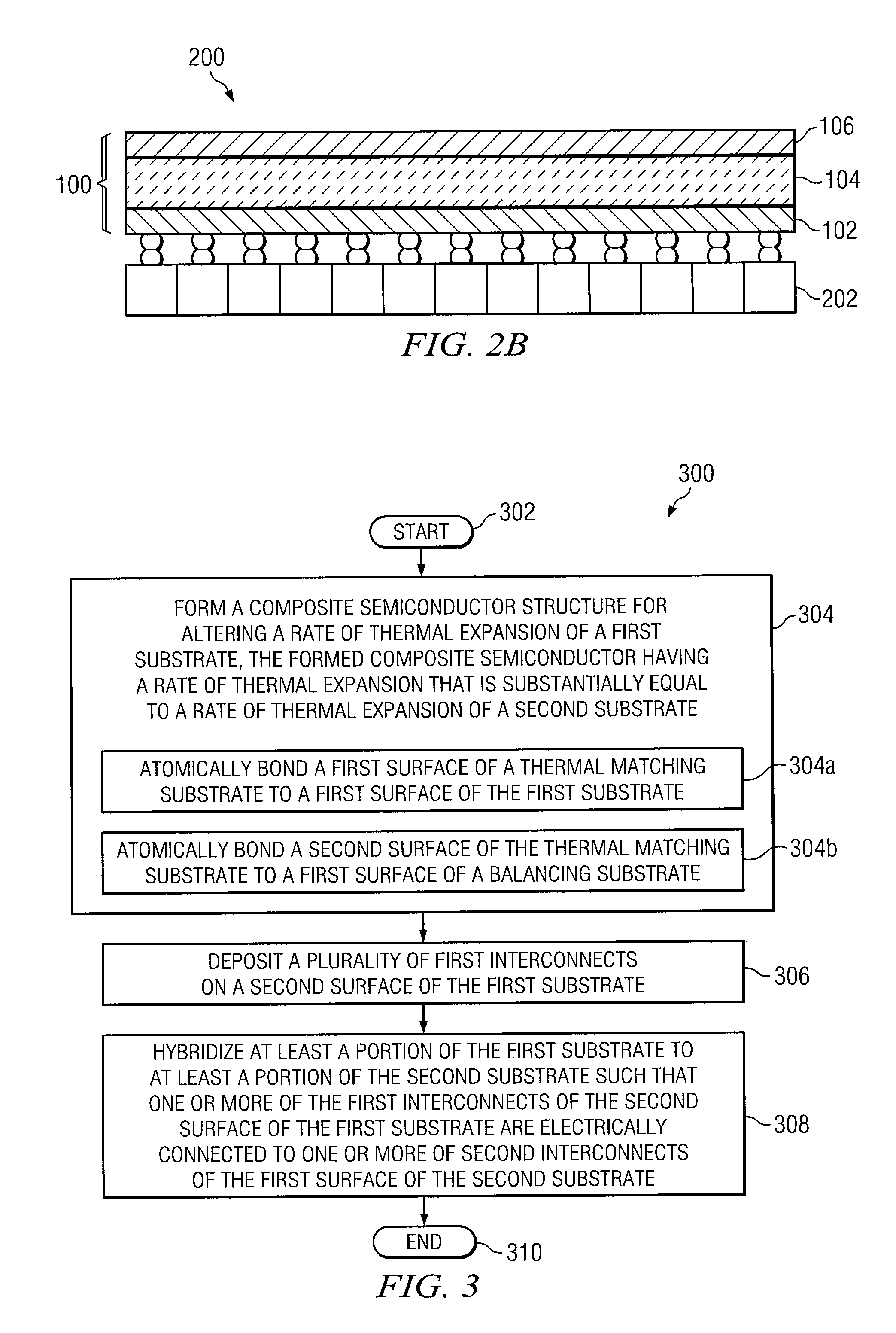
semiconductor structure for altering a rate of thermal expansion of a first substrate. The composite
semiconductor structure is formed by atomically bonding a first surface of a thermal matching substrate to a first surface of the first substrate and atomically bonding a second surface of the thermal matching substrate to a first surface of a balancing substrate. The thermal matching substrate is adapted to alter the rate of thermal expansion of the first substrate and the balancing substrate is adapted to substantially prevent warping of the composite semiconductor structure.
Because the technique for altering the rate of thermal expansion of a first substrate of certain embodiments of the present invention includes forming a composite semiconductor structure using atomic bonds (which are relatively insensitive to temperature changes), the composite semiconductor structure of certain embodiments of the present invention may be formed prior to elevated temperature hybridization. Thus, the first substrate may be thermally matched to a second substrate prior to elevated temperature hybridization and may remain thermally matched to the second substrate during elevated temperature hybridization. As a result, the technique for altering the rate of thermal expansion of a first substrate of certain embodiments of the present invention may allow for the formation of devices (e.g., SCAs for
image capture) having a first substrate (e.g., a ROIC device) hybridized at elevated temperature to the second substrate (e.g., a detector array), unlike certain conventional techniques.
Furthermore, even if thermal mismatch between the first and second substrate does not prevent hybridization of the first substrate to the second substrate (as discussed above), it may still be desirable to alter the rate of thermal expansion of the first substrate such that the rate of thermal expansion of the first substrate substantially matches the rate of thermal expansion of the second substrate (for the reasons discussed above). However, because certain conventional techniques do not allow for the altering of the rate of thermal expansion of the first substrate prior to elevated temperature hybridization, it may be necessary to alter the rate of thermal expansion of the first substrate subsequent to hybridization (e.g., by bonding the thermal matching substrate to the first substrate using an
epoxy). Because altering the rate of thermal expansion of the first substrate subsequent to hybridization is performed at the die level, which may be
time consuming and labor intensive, the cost associated with generating certain devices (e.g., sensor
chip arrays (SCAs) for
image capture) having a first substrate (e.g., including a ROIC device) hybridized to a second substrate (e.g., including a detector array) may increase.
Because the technique for altering the rate of thermal expansion of a first substrate of certain embodiments of the present invention includes forming a composite semiconductor structure using atomic bonds (which are relatively insensitive to temperature changes), the composite semiconductor structure of certain embodiments of the present invention may be formed prior to elevated temperature hybridization. Thus, the composite semiconductor structure of the present invention may be formed at the
wafer level (e.g., by atomically bonding a
wafer comprising a plurality of ROIC devices to a thermal matching substrate) as opposed to at the die level. In other words, in certain embodiments, the present invention provides for
wafer level thermal expansion matching using atomic bonding. The formed composite semiconductor structure may be diced into a plurality of dies (e.g., each including a single ROIC device), and each die may be hybridized at elevated temperature to a second substrate (e.g., a detector array) to form a device (e.g., a SCA). Forming the composite semiconductor structure of the present invention at the wafer level prior to hybridization may be less
time consuming and / or less labor intensive than bonding the thermal matching substrate to the first substrate at the die level subsequent to hybridization. Therefore, the technique for altering the rate of thermal expansion of a first substrate of certain embodiments of the present invention may decrease the cost associated with forming devices (e.g., SCAs for
image capture) having a first substrate (e.g., including a ROIC device) hybridized to a second substrate (e.g., including a detector array).

