Using interrupted through-silicon-vias in integrated circuits adapted for stacking

a technology of integrated circuits and silicon vias, applied in the direction of electrical equipment construction details, cable/conductor manufacturing, electrotherapy, etc., can solve the problems of tsvs having to be located symmetrically, stacking bussed memory chips remain,

Active Publication Date: 2011-03-03
MOSAID TECH
View PDF12 Cites 124 Cited by
  • Summary
  • Abstract
  • Description
  • Claims
  • Application Information

AI Technical Summary

Problems solved by technology

However, a problem remains in stacking bussed memory chips that are each indistinguishable from one another.
That is, the problem of uniquely identifying each chip so that commands such as read and write are only executed by a single chip in the stack.
This approach does not work in stacked memory devices which are connected only with continuous vertical TSVs.
A disadvantage of this solution is that TSVs must be located symmetrically about the axis of rotation of the chip, which is typically the geographical center of a rectangular die.
This reduces the flexibility in placement of TSVs and may lead to a die size penalty.
The serial point-to-point daisy-chained ring configuration has a disadvantage in that the ring cannot be completely connected using TSVs.
However, assuming all of the stacked memory devices are identical, the last device would have unconnected inputs to the downstream links to the controller.
These unconnected inputs may pick up random noise, thus causing unnecessary logic transitions, and thus unnecessary power dissipation, on each downstream link.

Method used


Image

  • Using interrupted through-silicon-vias in integrated circuits adapted for stacking
  • Using interrupted through-silicon-vias in integrated circuits adapted for stacking
  • Using interrupted through-silicon-vias in integrated circuits adapted for stacking

Examples


Embodiment Construction

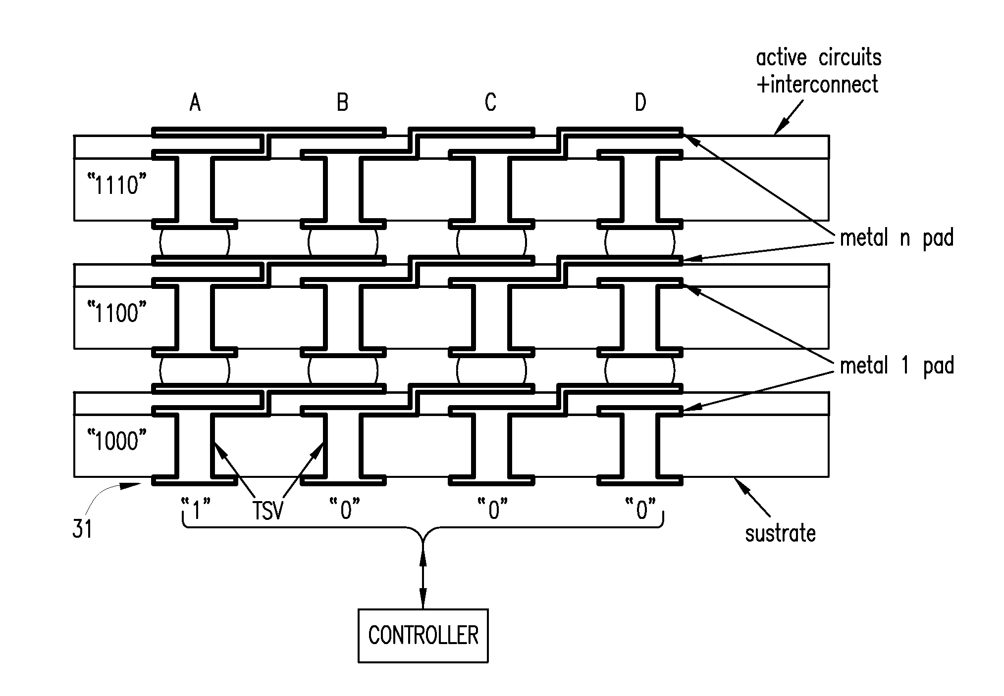
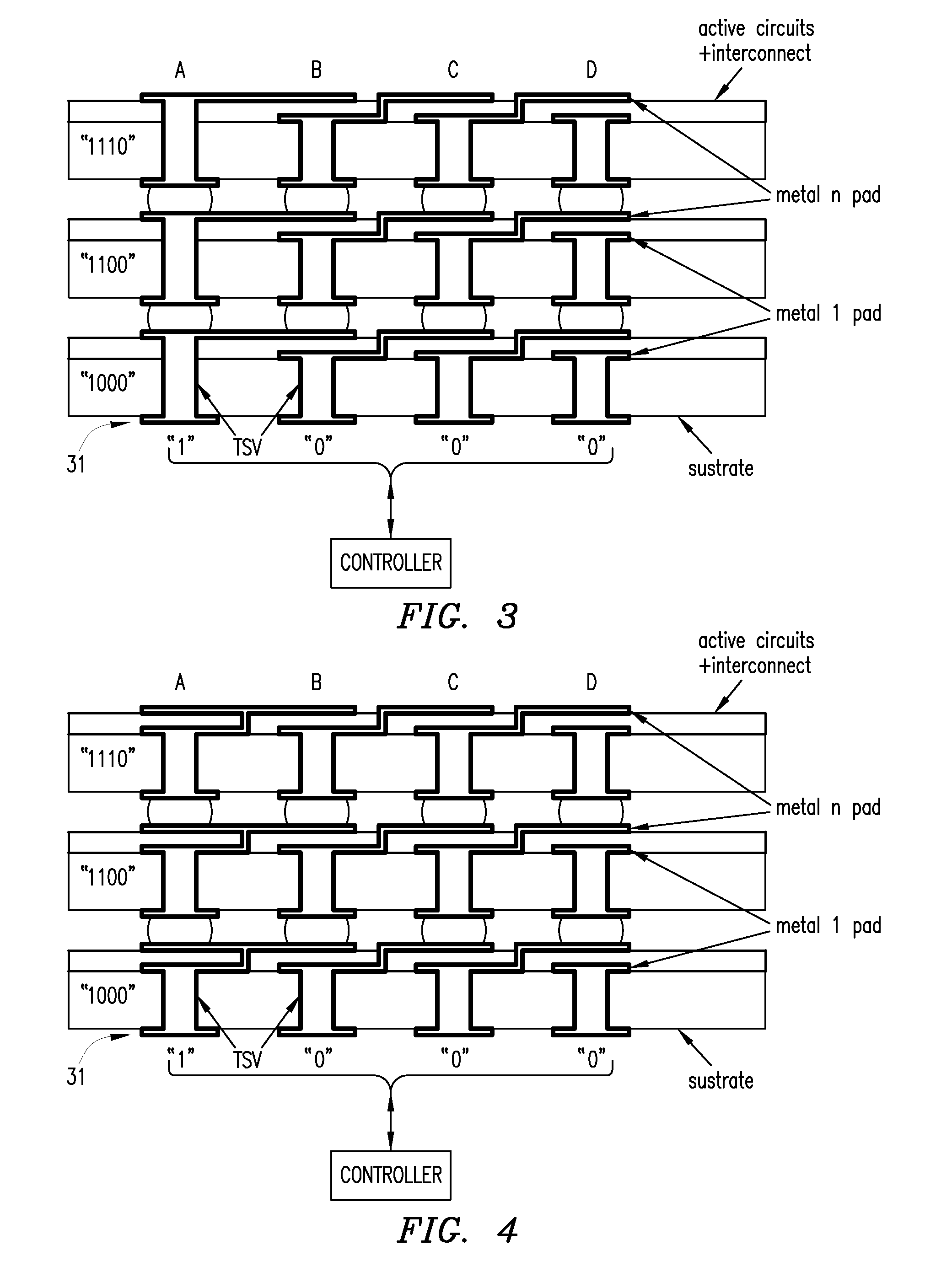
Example embodiments of the present work use interrupted TSVs that provide serial connections through successive integrated circuit die in a stack without the need for die rotation. With an interrupted TSV, the connection between bottom pad and top pad is broken to allow connections other than direct (uninterrupted) vertical connections.

FIG. 3 shows an example of stacked chips interconnected using interrupted TSVs according to the present work to provide connections that are not direct vertical connections. The TSVs in position A are conventional uninterrupted vertical connections between a pad on the bottom surface of the die and the top metal layer, while the TSVs in positions B, C, and D are interrupted TSVs.

Within the active circuit and interconnect region of the chip there may be many conductive layers. Modern logic processes have 9 layers of metal interconnect or even more. The top metal layer is indicated here as metal n and the bottom layer as metal 1. In addition connections...


PUM


Abstract

In an integrated circuit (IC) adapted for use in a stack of interconnected ICs, interrupted through-silicon-vias (TSVs) are provided in addition to uninterrupted TSVs. The interrupted TSVs provide signal paths other than common parallel paths between the ICs of the stack. This permits IC identification schemes and other functionalities to be implemented using TSVs, without requiring angular rotation of alternate ICs of the stack.

Description

FIELDThe present work relates generally to integrated circuits and, more particularly, to stacked arrangements of interconnected integrated circuits.BACKGROUNDThrough Silicon Via (TSV) technology is an emerging solution for connection of stacked semiconductor integrated circuit (IC) chips. Very wide busses are possible because the TSV density can be much higher than conventional pads for wire bonding. Normal bonding pads for wire bonds have planar dimensions of around 100 um while TSVs may be 10 um or even smaller. Connecting a bus between a number of stacked chips is straightforward because the connection is made vertically between each chip in a stack of chips. FIG. 1 shows the cross section of a TSV structure in a single integrated circuit die before wafer stacking. The TSV extends from the bottom of the chip through the silicon substrate and through the layers of active circuitry and interconnect. A pad is located at the top and bottom surface of the die electrically connected t...

Claims


Application Information

Patent Timeline
Patent Type & Authority Applications(United States)
IPC IPC(8): H03K17/00H01L23/48H01L23/488H01L23/538H01L21/60H01L21/768
CPCG11C5/02H01L24/03H01L23/481H01L23/5286H01L23/544H01L24/16H01L25/0657H01L2223/54433H01L2223/5444H01L2225/06513H01L2225/06527H01L2225/06541H01L2225/06562H01L2924/01078H01L2924/01055H01L21/02697H01L21/82H03K17/00H01L2224/0401H01L2224/06181G11C5/06H01L2924/14H01L2924/00H01L23/488H01L23/50H01L2225/0652H01L2225/06548
Inventor GILLINGHAM, PETER B.
Owner MOSAID TECH
Why Eureka
Try Eureka