Electronic detonator control chip

a control chip and detonator technology, applied in the direction of electric fuzes, instruments, lighting and heating apparatus, etc., can solve the problems of low precision but, unchangeable delay time, heavy metal dispersion, etc., to improve the flexibility of blasting network design, simplify construction complexity, and reduce the quantity of registers

Active Publication Date: 2011-03-10
BEIJING EBTECH TECHNOLOGY CO LTD
View PDF6 Cites 38 Cited by
  • Summary
  • Abstract
  • Description
  • Claims
  • Application Information

AI Technical Summary

Benefits of technology

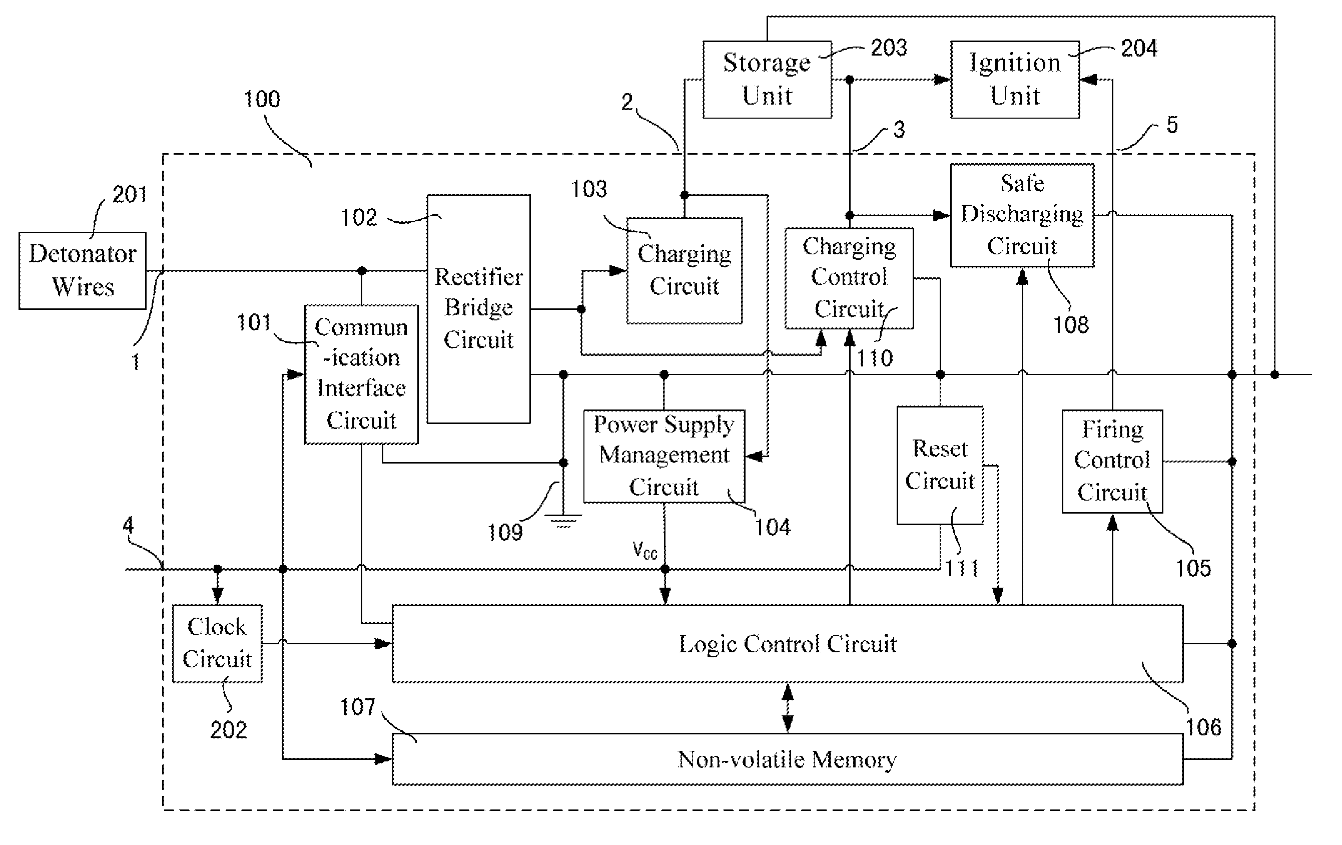
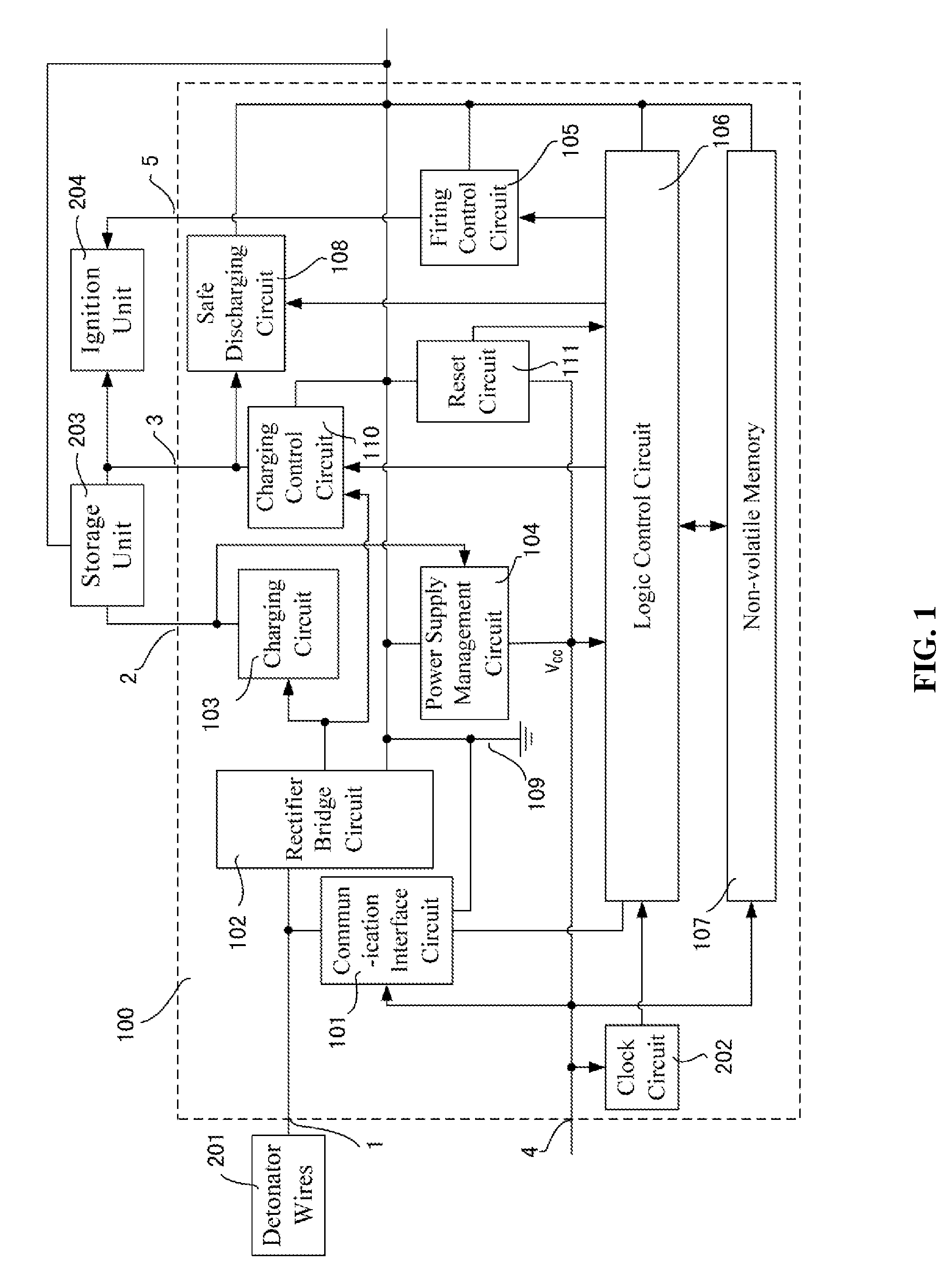
[0010]In the electronic detonator control chip, one end of the rectifier bridge circuit is connected to the communication interface circuit, forming at least one first pin extending to the exterior of the chip; one end of the rectifier bridge circuit leads to the charging circuit and the charging control circuit, supplying power to the both above; the other end of the rectifier bridge circuit is grounded. The rectifier bridge circuit realizes non-polarity connection of the electronic detonator wires and eliminates the risk of the damage to the electronic detonator control chip caused by reverse connection of the electronic detonator wires, which makes the use of the electronic detonator easier and more secure.
[0069]A presettable down-counter is a better choice for the programmable delay module. After receiving the delay-time data included in the delay-time-writing instruction, the CPU can directly write the delay-time data into the presettable down-counter via the internal bus, reducing the registers' quantity demanded for temporary data in the CPU. Adopting the presettable down-counter, when it counts down to zero which means that the delay time has arrived, the delay-time data included in the delay-time-writing instruction can be directly adopted as the data written into the down-counter without any transformation. On the contrary, if a presettable up-counter is adopted, the data written into the up-counter is needed to be calculated according to the delay-time data included in the delay-time-writing instruction. The calculation process goes as follows: according to theory that the delay time arrives when the up-counter counts up to its upper limit, the data written into the up-counter is gained by subtracting the delay-time data included in the delay-time-writing instruction from the upper limit of the presettable up-counter. In summary, the adoption of the down-counter makes the design simpler.

Problems solved by technology

A delay element is used to realize the function of delay of traditional electric detonators, which results in not only low precision but also unchangeable delay time.
In addition, since the delay element contains delay composition and heavy metal such as lead, the use of traditional electric detonators can lead to dispersion of the heavy metal and the burning of the delay composition, both causing environment pollution.
Further, public safety problems may arise from the traditional electric detonator.
On the one hand, the process of detonation of a traditional electric detonator is uncontrollable because the detonation process starts immediately once the detonator is powered, and the process is irreversible and can not be interrupted or stopped in case of emergency.
On the other hand, since the ignition unit is connected directly to detonator wires, external interferences such as static electricity, radio frequency, stray current and so on may directly affect the security of the detonator during production, storage and use.
Under traditional management system and technology, the traditional detonators can not be easily managed and controlled and sometimes be accessible to unauthorized persons.
Lost detonators can definitely do harm to social security.
However, the physical process of tagging on the shell may reduce the safety of detonator production, and further, coding and tagging still cannot solve the controllability problem in detonator management.

Method used


Image

  • Electronic detonator control chip
  • Electronic detonator control chip
  • Electronic detonator control chip

Examples


first embodiment

[0138]As the charging control circuit 1101, as shown in FIG. 10, the charging control circuit 1101 includes a PMOS transistor 705, a PMOS transistor 706, a PMOS transistor 707, an NMOS transistor 807, an NMOS transistor 808, an NMOS transistor 809, a resistor 307, and a diode 406. The detailed connection is described as follows:[0139]The source and the substrate of the PMOS transistor 705 are connected to the power supply management circuit 104, the grid of the PMOS transistor 705, the grid of the NMOS transistor 807 and the grid of the NMOS transistor 808 are connected to the logic control circuit 106 together. The drain of the PMOS transistor 705, the drain of the NMOS transistor 807 and the grid of the NMOS transistor 809 connect together. The source and the substrate of the PMOS transistor 706, and the source and the substrate of the PMOS transistor 707 connect together, and are connected to the rectifier bridge circuit 102 together. The grid of the PMOS transistor 706, the drai...

second embodiment

[0140]As the charging control circuit 1101, as shown in FIG. 11, the charging control circuit 1101 includes a PMOS transistor 705, a PMOS transistor 706, a PMOS transistor 707, an NMOS transistor 807, an NMOS transistor 808, an NMOS transistor 809, a resistor 307, and a diode 406. The detailed connection is described as follows:[0141]The source and the substrate of the PMOS transistor 705 are connected to the power supply management circuit 104. The grid of the PMOS transistor 705, the grid of the NMOS transistor 807 and the grid of the NMOS transistor 808 are connected to the logic control circuit 106 together. The drain of the PMOS transistor 705, the drain of the NMOS transistor 807 and the grid of the NMOS transistor 809 connect together. The source and the substrate of the PMOS transistor 706, the substrate of the PMOS transistor 707 and one end of the resistor 307 are connected to the rectifier bridge circuit 102 together; while the other end of the resistor 307 is connected t...

third embodiment

[0142]As the charging control circuit 1101, as shown in FIG. 12, the charging control circuit 1101 includes a PMOS transistor 705, a PMOS transistor 706, a PMOS transistor 707, an NMOS transistor 807, an NMOS transistor 808, an NMOS transistor 809, a resistor 307, and a diode 406. The detailed connection is described as follows:[0143]The source and the substrate of the PMOS transistor 705 are connected to the power supply management circuit 104; the grid of the PMOS transistor 705, the grid of the NMOS transistor 807, and the grid of the NMOS transistor 808 are connected to the logic control circuit 106 together; the drain of the PMOS transistor 705, the drain of the NMOS transistor 807, and the grid of the NMOS transistor 809 connect together. The source and the substrate of the PMOS transistor 706, and the source and the substrate of the PMOS transistor 707 are connected to one end of the resistor 307 together, while the other end of the resistor 307 is connected to the rectifier ...


PUM


Abstract

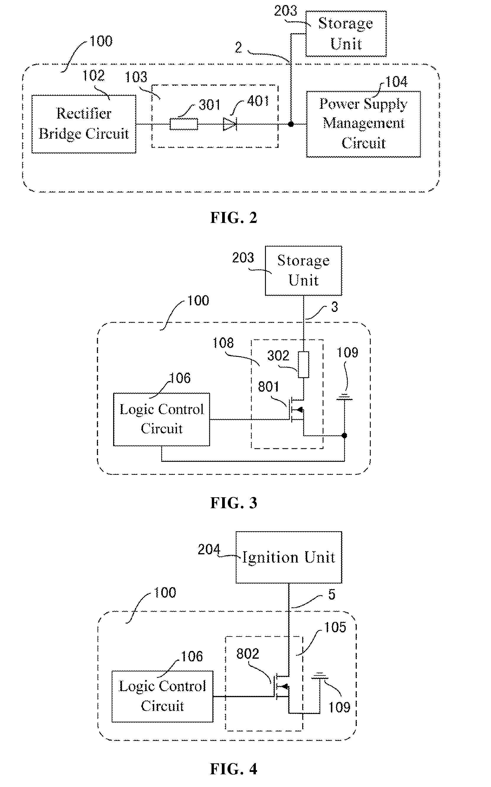
An electronic detonator control chip (100) includes a communication interface circuit (101), a rectification bridge circuit (102), a charging circuit (103), a charging control circuit (110), a power management circuit (104), a firing control circuit (105), a logic control circuit (106), a non-volatile memory (107), a reset circuit (111), a safe discharging circuit (108), and a clock circuit (202). Wherein, the communication interface circuit (101) includes a data modulation module (210) and a data demodulation module (211) including two data demodulation circuits (212). The logic control circuit (106) further includes a programmable delay module (281), an input / out interface (282), a serial communication interface (283), a prescaler (284), a CPU (285), and so on. Therefore, the electronic detonator control chip provided by the invention enables to realize the functions of two-wire non-polarity connection, bidirectional communication with a detonation equipment external of the electronic detonator control chip, ID card inside the detonator, control of the detonation process and online program of the delay time and so on.

Description

CROSS-REFERENCE TO RELATED APPLICATIONS[0001]This application is a continuation of International Patent Application No. PCT / CN09 / 71504 filed Apr. 27, 2009 and designating the United States, which application in turn claims priority of Chinese Patent Application No. 200820111269.7 filed Apr. 28, 2008, Chinese Patent Application No. 200820115927.X filed Jun. 4, 2008, Chinese Patent Application No. 200820136278.1 filed Sep. 24, 2008, Chinese Patent Application No. 200810211374.2 filed Sep. 24, 2008, and Chinese Patent Application No. 200810172410.9 filed Nov. 7, 2008. The disclosures of each of the foregoing applications are hereby incorporated herein by reference in their respective entireties, for all purposes.TECHNICAL FIELD[0002]The present invention relates to the field of the manufacturing technology of initiating explosive device, in particular to an electronic detonator control chip.BACKGROUND OF THE INVENTION[0003]A delay element is used to realize the function of delay of tra...

Claims


Application Information

Patent Timeline
Patent Type & Authority Applications(United States)
IPC IPC(8): F42B3/10
CPCF42C11/065F42B3/122
Inventor YAN, JINGLONGLIU, XINGLI, FENGGUOLAI, HUAPINGZHANG, XIANYU
Owner BEIJING EBTECH TECHNOLOGY CO LTD
Why Eureka
Try Eureka