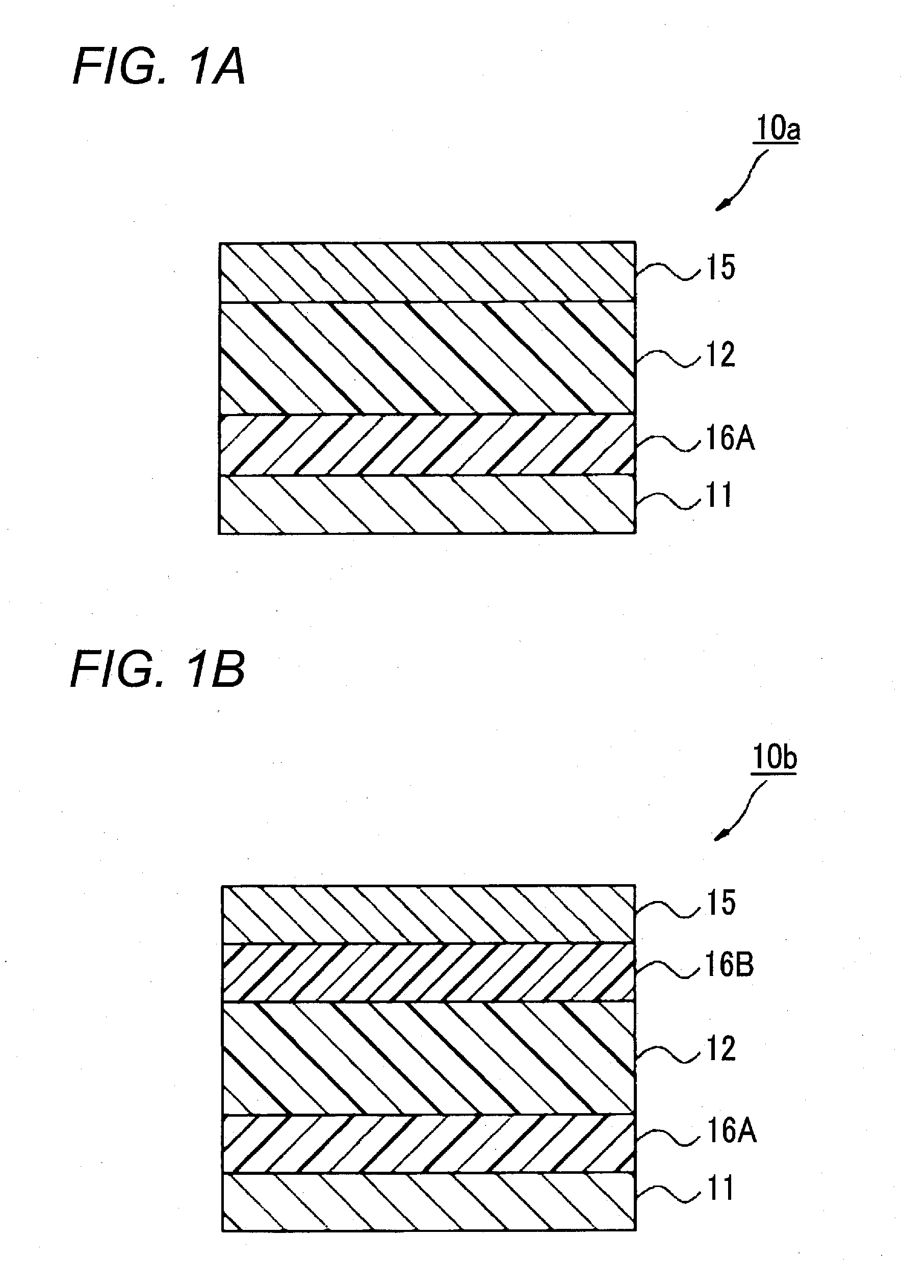
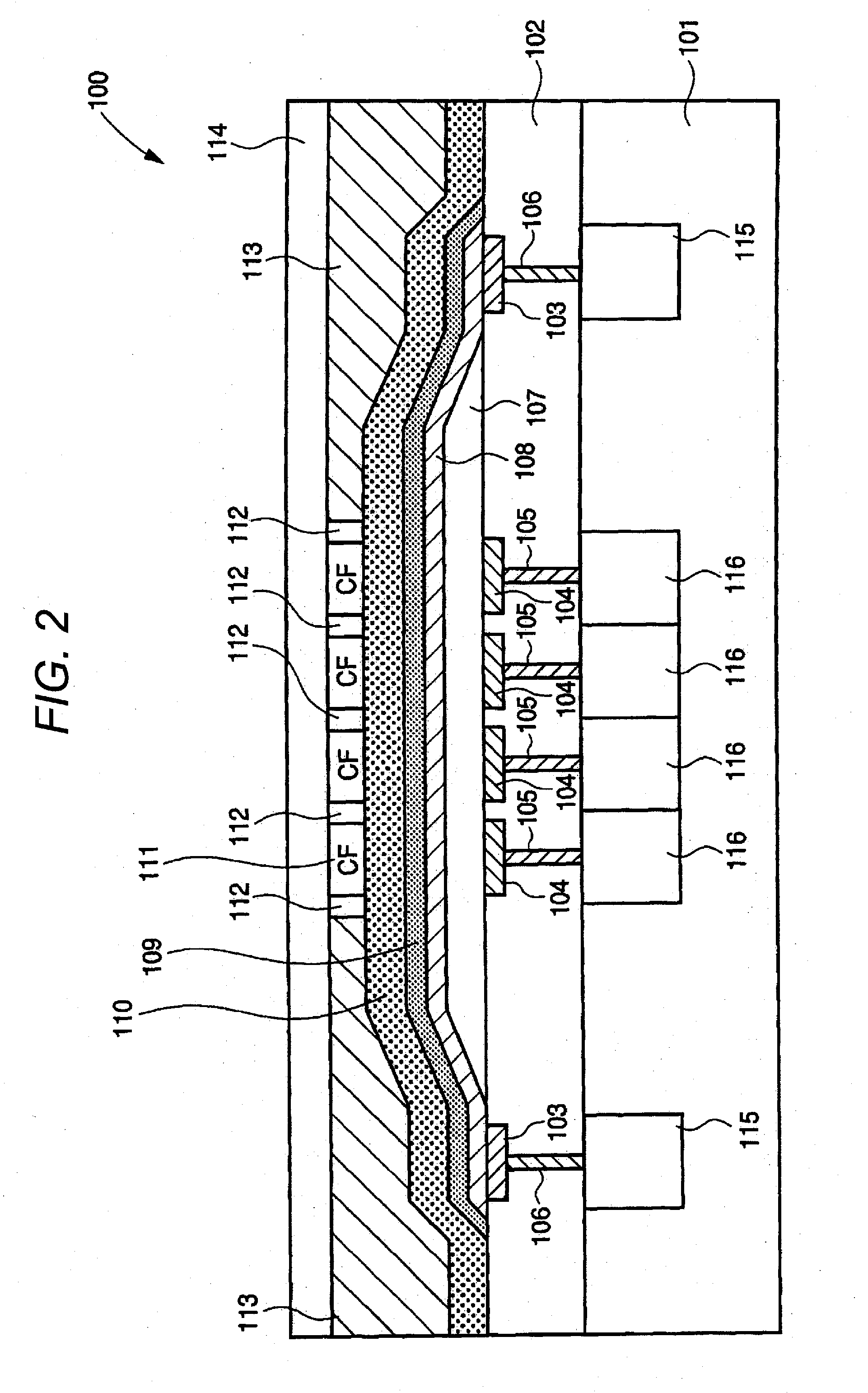
Photoelectric conversion material, film containing the material, photoelectric conversion device, production method thereof, photosensor, imaging device and their use methods

a technology of photoelectric conversion and film containing material, which is applied in the direction of methine/polymethine dye, optical radiation measurement, instruments, etc., can solve the problems of reducing the aperture ratio and the light collection efficiency, and the failure of light to transmit through the color filter is not utilized, etc., to achieve high heat resistance, high sensitivity, and high speed responsivity

Active Publication Date: 2011-03-10
FUJIFILM CORP
View PDF12 Cites 13 Cited by
  • Summary
  • Abstract
  • Description
  • Claims
  • Application Information

AI Technical Summary

Benefits of technology

[0018]An object of the present invention is to provide a photoelectric conversion device and a solid-state imaging device, in which sufficiently high sensitivity and high heat resistance are obtained and high-speed responsivity is exhibited.
[0019]In an organic photoelectric conversion device, for realizing high photoelectric conversion efficiency, low dark current and high-speed responsivity, the organic photoelectric conversion film used preferably satisfies the following requirements.
[0020]1. In terms of high efficiency and high-speed response, the signal charge after dissociation of an exciton needs to be swiftly transmitted to both electrodes without loss. High mobility and high charge transportability with a small number of carrier trapping sites are necessary.

Problems solved by technology

In this single-plate solid-state imaging device, since the color filter transmits only light at a limited wavelength, light failed in transmitting through the color filter is not utilized and the light utilization efficiency is bad.
Also, in recent years, fabrication of a multipixel device is proceeding, and the pixel size and in turn, the area of a photodiode part become small, which brings about problems of reduction in the aperture ratio and reduction in the light collection efficiency.
However, such a system is disadvantageous in that the color separation is poor, because the absorption range is overlapped among respective portions in the depth direction of Si and the spectroscopic property is bad.
In an attempt to increase the photoelectric conversion efficiency by the introduction of pn-junction or bulk heterojunction structure, an increase in the dark current often becomes a problem.
In the case of employing the method above, what materials are combined is important and in particular, when reduction in the dark time noise is intended, this is difficult to achieve by conventionally reported combinations of materials.
In use as a solid-state imaging device, all of high photoelectric conversion efficiency, low dark current and high response speed need to be satisfied, but there has not been specifically disclosed what an organic photoelectric conversion material or a device structure satisfies this requirement.
A photoelectric conversion film containing fullerenes is described in Patent Document 3, but only by fullerenes, it is impossible to satisfy all of the above-described high photoelectric conversion efficiency, low dark current and high response speed.

Method used


Image

  • Photoelectric conversion material, film containing the material, photoelectric conversion device, production method thereof, photosensor, imaging device and their use methods
  • Photoelectric conversion material, film containing the material, photoelectric conversion device, production method thereof, photosensor, imaging device and their use methods
  • Photoelectric conversion material, film containing the material, photoelectric conversion device, production method thereof, photosensor, imaging device and their use methods

Examples


example 1

[0204]

(Synthesis of Compound 1a)

[0205]To 10 ml of dehydrated xylene, 4.0 g of N-phenyl-2-naphthylamine (produced by Tokyo Chemical Industry Co., Ltd.), 4.0 g of methyl 6-bromo-2-naphthoate (produced by Wako Pure Chemical Industries, Ltd.), 170 mg of palladium acetate, 590 mg of triphenylphosphine and 9.8 g of cesium carbonate were added, followed by refluxing for 3 hours. The reaction mixture was suction-filtered and after distilling off the solvent by an evaporator, the residue was purified on a silica gel column (developing solvent: toluene). The solvent was distilled off to obtain 6.2 g of Compound (1a).

(Synthesis of Compound 1b)

[0206]To 30 ml of dehydrated toluene, 23.6 ml of SMEAH (a toluene solution (about 70%) of sodium hydrogenated bis(2-methoxyethoxy)aluminum (produced by Wako Pure Chemical Industries, Ltd.)) was added, and after adjusting the inner temperature to 0° C. in an ice bath, a solution obtained by dissolving 9.9 ml of 1-methylpiperazine in 17 ml of dehydrated tol...

example 2

Synthesis of Compound (2)

[0215]Compound (2b) and Compound (2) were synthesized in the same manner as in Example 1 except for changing N-phenyl-2-naphthylamine to 2,2′-dinaphthylamine (produced by Tokyo Chemical Industry Co., Ltd.).

[0216]1H NMR (CDCl3) δ: 7.39 (4H, dd), 7.43-7.47 (4H, m), 7.58-7.66 (5H, m), 7.80-7.89 (6H, m), 8.24 (1H, s), 10.10 (1H, s).

[0217]1H NMR (CDCl3) δ: 7.39-7.49 (8H, m), 7.60-7.74 (7H, m), 7.84 (4H, d), 7.90 (1H, d), 8.12 (3H, m), 8.53 (2H, d), 8.60 (1H, d), 9.04 (1H, s).

[0218]Molecular weight: 601.69

[0219]The melting point of Compound (2) was measured in the same manner as in Example 1 and found to be 309° C.

[0220]The absorption spectrum (in a chloroform solution) of Compound (2) was measured in the same manner as in Example 1, as a result, the peak wavelength was 548 nm and the molar extinction coefficient at this wavelength was 54,000 M−1 cm−1.

[0221]A solid-state imaging device including a photoelectric conversion device was fabricated in the same manner a...

example 3

Synthesis of Compound (3)

[0222]Compound (3) was synthesized in the same manner as in Example 1 except for changing benzoindandione to indandione.

[0223]1H NMR (CDCl3) δ: 7.18 (1H, t), 7.23 (1H, d), 7.32-7.49 (7H, d), 7.57-7.68 (4H, m), 7.79-7.88 (5H, m), 8.02 (3H, m), 8.53 (1H, d), 8.92 (1H, s).

[0224]Molecular weight: 501.57

[0225]The melting point of Compound (3) was measured in the same manner as in Example 1 and found to be 253° C.

[0226]The absorption spectrum (in a chloroform solution) of Compound (3) was measured in the same manner as in Example 1, as a result, the peak wavelength was 514 nm and the molar extinction coefficient at this wavelength was 40,000 M−1 cm−1.

[0227]A solid-state imaging device including a photoelectric conversion device was fabricated in the same manner as in Example 1 except for changing Compound (1) in the photoelectric conversion layer to Compound (3).


PUM

PropertyMeasurementUnit
distanceaaaaaaaaaa
distanceaaaaaaaaaa
distanceaaaaaaaaaa

Abstract

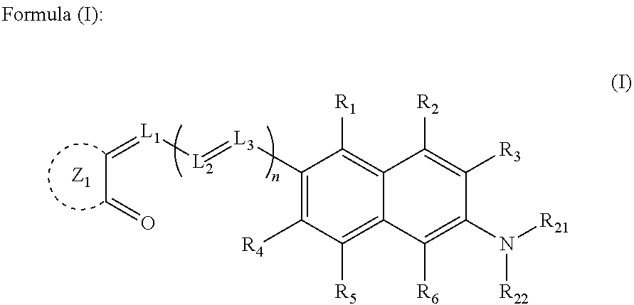
A compound represented by the following formula (I), and a photoelectric conversion device containing the compound:wherein Z1 is a ring containing two carbon atoms and represents a 5-membered ring, a 6-membered ring or a condensed ring containing at least either a 5-membered ring or a 6-membered ring, each of L1, L2 and L3 independently represents an unsubstituted methine group or a substituted methine group, n represents an integer of 0 or more, each of R1, R2, R3, R4, R5 and R6 independently represents a hydrogen atom or a substituent, R1 and R2, R2 and R3, R4 and R5, or R5 and R6 may be combined with each other to form a ring, and each of R21 and R22 independently represents a substituted aryl group, an unsubstituted aryl group, a substituted heteroaryl group or an unsubstituted heteroaryl group, provided that the case where both R21 and R22 are an unsubstituted phenyl group is excluded.

Description

BACKGROUND OF THE INVENTION[0001]1. Field of the Invention[0002]The present invention relates to a novel compound useful as a photoelectric conversion device material, a film containing the material, a photoelectric conversion device, a production method thereof, a photosensor, an imaging device and their use methods.[0003]2. Description of the Related Art[0004]Conventional photosensors in general are a device fabricated by forming a photodiode (PD) in a semiconductor substrate such as silicon (Si). As for the solid-state imaging device, there is widely used a flat solid-state imaging device where PD are two-dimensionally arrayed in a semiconductor substrate and a signal according to a signal charge generated by photoelectric conversion in each PD is read out through a CCD or CMOS circuit.[0005]The method for realizing a color solid-state imaging device is generally fabrication of a structure where on the light incident surface side of the flat solid-state imaging device, a color fi...

Claims


Application Information

Patent Timeline
Patent Type & Authority Applications(United States)
IPC IPC(8): H01L31/04C07C211/58C07C211/61C07D213/74C07D221/18H01L31/18
CPCC07C223/06C09B57/008C07C2102/08C07C2103/14C07C2103/18C07C2103/24C07C2103/26C07C2103/50C07D209/86C07D213/74C07D219/02C07D221/18C07D223/14C07D239/62C07D239/66C07D307/66C07D333/36C07D495/04H01L27/307H01L51/006H01L51/4253Y02E10/549C09B23/04C07C225/22C07C2602/08C07C2603/14C07C2603/18C07C2603/24C07C2603/26C07C2603/50H10K39/32H10K85/633H10K30/30G01J1/04H01L31/04Y02E10/50
Inventor HAMANO, MITSUMASAYOFU, KATSUYUKIMITSUI, TETSURONOMURA, KIMIATSU
Owner FUJIFILM CORP
Why Eureka
Try Eureka